MC908MR32CFUE Freescale Semiconductor, MC908MR32CFUE Datasheet - Page 209
MC908MR32CFUE
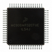
Manufacturer Part Number
MC908MR32CFUE
Description
IC MCU 8MHZ 32K FLASH 64-QFP
Manufacturer
Freescale Semiconductor
Series
HC08r
Datasheet
1.MC908MR16CFUE.pdf
(282 pages)
Specifications of MC908MR32CFUE
Core Processor
HC08
Core Size
8-Bit
Speed
8MHz
Connectivity
SCI, SPI
Peripherals
LVD, POR, PWM
Number Of I /o
44
Program Memory Size
32KB (32K x 8)
Program Memory Type
FLASH
Ram Size
768 x 8
Voltage - Supply (vcc/vdd)
4.5 V ~ 5.5 V
Data Converters
A/D 10x10b
Oscillator Type
Internal
Operating Temperature
-40°C ~ 85°C
Package / Case
64-QFP
Processor Series
HC08MR
Core
HC08
Data Bus Width
8 bit
Data Ram Size
768 B
Interface Type
SCI/SPI
Maximum Clock Frequency
8.2 MHz
Number Of Programmable I/os
44
Number Of Timers
6
Operating Supply Voltage
0 V to 5 V
Maximum Operating Temperature
+ 85 C
Mounting Style
SMD/SMT
Development Tools By Supplier
FSICEBASE, M68CBL05CE
Minimum Operating Temperature
- 40 C
On-chip Adc
10-ch x 10-bit
Lead Free Status / RoHS Status
Lead free / RoHS Compliant
Eeprom Size
-
Lead Free Status / Rohs Status
Lead free / RoHS Compliant
Available stocks
Company
Part Number
Manufacturer
Quantity
Price

Company:
Part Number:
MC908MR32CFUE
Manufacturer:
Freescale Semiconductor
Quantity:
10 000
Part Number:
MC908MR32CFUE
Manufacturer:
NXP/恩智浦
Quantity:
20 000


The SPI has limited inter-integrated circuit (I
single-master environment. To communicate with I
when the SPWOM bit in the SPI control register is set. In I
are connected to a bidirectional pin from the I
15.11.1 MISO (Master In/Slave Out)
MISO is one of the two SPI module pins that transmits serial data. In full duplex operation, the MISO pin
of the master SPI module is connected to the MISO pin of the slave SPI module. The master SPI
simultaneously receives data on its MISO pin and transmits data from its MOSI pin.
Slave output data on the MISO pin is enabled only when the SPI is configured as a slave. The SPI is
configured as a slave when its SPMSTR bit is logic 0 and its SS pin is at logic 0. To support a
multiple-slave system, a logic 1 on the SS pin puts the MISO pin in a high-impedance state.
When enabled, the SPI controls data direction of the MISO pin regardless of the state of the data direction
register of the shared
I/O port.
15.11.2 MOSI (Master Out/Slave In)
MOSI is one of the two SPI module pins that transmits serial data. In full-duplex operation, the MOSI pin
of the master SPI module is connected to the MOSI pin of the slave SPI module. The master SPI
simultaneously transmits data from its MOSI pin and receives data on its MISO pin.
When enabled, the SPI controls data direction of the MOSI pin regardless of the state of the data direction
register of the shared I/O port.
15.11.3 SPSCK (Serial Clock)
The serial clock synchronizes data transmission between master and slave devices. In a master MCU,
the SPSCK pin is the clock output. In a slave MCU, the SPSCK pin is the clock input. In full-duplex
operation, the master and slave MCUs exchange a byte of data in eight serial clock cycles.
When enabled, the SPI controls data direction of the SPSCK pin regardless of the state of the data
direction register of the shared I/O port.
15.11.4 SS (Slave Select)
The SS pin has various functions depending on the current state of the SPI. For an SPI configured as a
slave, the SS is used to select a slave. For CPHA = 0, the SS is used to define the start of a transmission.
See
toggled high and low between each byte transmitted for the CPHA = 0 format. However, it can remain low
between transmissions for the CPHA = 1 format. See
Freescale Semiconductor
15.5 Transmission
MASTER SS
MISO/MOSI
SLAVE SS
SLAVE SS
CPHA = 0
CPHA = 1
Formats. Since it is used to indicate the start of a transmission, the SS must be
MC68HC908MR32 • MC68HC908MR16 Data Sheet, Rev. 6.1
BYTE 1
Figure 15-13. CPHA/SS Timing
2
C) capability (requiring software support) as a master in a
2
C peripheral and through a pullup resistor to V
2
C peripherals, MOSI becomes an open-drain output
Figure
BYTE 2
2
C communication, the MOSI and MISO pins
15-13.
BYTE 3
DD
I/O Signals
.
209
Related parts for MC908MR32CFUE
Image
Part Number
Description
Manufacturer
Datasheet
Request
R

Part Number:
Description:
Manufacturer:
Freescale Semiconductor, Inc
Datasheet:
Part Number:
Description:
Manufacturer:
Freescale Semiconductor, Inc
Datasheet:
Part Number:
Description:
Manufacturer:
Freescale Semiconductor, Inc
Datasheet:
Part Number:
Description:
Manufacturer:
Freescale Semiconductor, Inc
Datasheet:
Part Number:
Description:
Manufacturer:
Freescale Semiconductor, Inc
Datasheet:
Part Number:
Description:
Manufacturer:
Freescale Semiconductor, Inc
Datasheet:
Part Number:
Description:
Manufacturer:
Freescale Semiconductor, Inc
Datasheet:
Part Number:
Description:
Manufacturer:
Freescale Semiconductor, Inc
Datasheet:
Part Number:
Description:
Manufacturer:
Freescale Semiconductor, Inc
Datasheet:
Part Number:
Description:
Manufacturer:
Freescale Semiconductor, Inc
Datasheet:
Part Number:
Description:
Manufacturer:
Freescale Semiconductor, Inc
Datasheet:
Part Number:
Description:
Manufacturer:
Freescale Semiconductor, Inc
Datasheet:
Part Number:
Description:
Manufacturer:
Freescale Semiconductor, Inc
Datasheet:
Part Number:
Description:
Manufacturer:
Freescale Semiconductor, Inc
Datasheet:
Part Number:
Description:
Manufacturer:
Freescale Semiconductor, Inc
Datasheet: