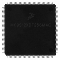
MC9S12XDT256MAG Freescale Semiconductor, MC9S12XDT256MAG Datasheet - Page 528

MC9S12XDT256MAG
Manufacturer Part Number
MC9S12XDT256MAG
Description
IC MCU 256K FLASH 144-LQFP
Manufacturer
Freescale Semiconductor
Series
HCS12r
Datasheet
1.MC9S12XD64CAA.pdf
(1348 pages)
Specifications of MC9S12XDT256MAG
Core Processor
HCS12X
Core Size
16-Bit
Speed
80MHz
Connectivity
CAN, EBI/EMI, I²C, IrDA, LIN, SCI, SPI
Peripherals
LVD, POR, PWM, WDT
Number Of I /o
119
Program Memory Size
256KB (256K x 8)
Program Memory Type
FLASH
Eeprom Size
4K x 8
Ram Size
16K x 8
Voltage - Supply (vcc/vdd)
2.35 V ~ 5.5 V
Data Converters
A/D 24x10b
Oscillator Type
External
Operating Temperature
-40°C ~ 125°C
Package / Case
144-LQFP
Processor Series
S12XD
Core
HCS12
Data Bus Width
16 bit
Data Ram Size
16 KB
Interface Type
CAN/I2C/SCI/SPI
Maximum Clock Frequency
40 MHz
Number Of Programmable I/os
119
Number Of Timers
12
Operating Supply Voltage
0 V to 5.5 V
Maximum Operating Temperature
+ 125 C
Mounting Style
SMD/SMT
3rd Party Development Tools
EWHCS12
Development Tools By Supplier
EVB9S12XDP512E
Minimum Operating Temperature
- 40 C
On-chip Adc
2 (24-ch x 10-bit)
Lead Free Status / RoHS Status
Lead free / RoHS Compliant
Available stocks
Company
Part Number
Manufacturer
Quantity
Price
Company:
Part Number:
MC9S12XDT256MAG
Manufacturer:
Freescale Semiconductor
Quantity:
10 000
- Current page: 528 of 1348
- Download datasheet (8Mb)
Chapter 12 Serial Peripheral Interface (S12SPIV4)
12.4
The SPI module allows a duplex, synchronous, serial communication between the MCU and peripheral
devices. Software can poll the SPI status flags or SPI operation can be interrupt driven.
The SPI system is enabled by setting the SPI enable (SPE) bit in SPI control register 1. While SPE is set,
the four associated SPI port pins are dedicated to the SPI function as:
The main element of the SPI system is the SPI data register. The 8-bit data register in the master and the
8-bit data register in the slave are linked by the MOSI and MISO pins to form a distributed 16-bit register.
When a data transfer operation is performed, this 16-bit register is serially shifted eight bit positions by the
S-clock from the master, so data is exchanged between the master and the slave. Data written to the master
SPI data register becomes the output data for the slave, and data read from the master SPI data register after
a transfer operation is the input data from the slave.
A read of SPISR with SPTEF = 1 followed by a write to SPIDR puts data into the transmit data register.
When a transfer is complete and SPIF is cleared, received data is moved into the receive data register. This
8-bit data register acts as the SPI receive data register for reads and as the SPI transmit data register for
writes. A single SPI register address is used for reading data from the read data buffer and for writing data
to the transmit data register.
The clock phase control bit (CPHA) and a clock polarity control bit (CPOL) in the SPI control register 1
(SPICR1) select one of four possible clock formats to be used by the SPI system. The CPOL bit simply
selects a non-inverted or inverted clock. The CPHA bit is used to accommodate two fundamentally
different protocols by sampling data on odd numbered SCK edges or on even numbered SCK edges (see
Section 12.4.3, “Transmission
The SPI can be configured to operate as a master or as a slave. When the MSTR bit in SPI control register1
is set, master mode is selected, when the MSTR bit is clear, slave mode is selected.
528
•
•
•
•
Slave select (SS)
Serial clock (SCK)
Master out/slave in (MOSI)
Master in/slave out (MISO)
Functional Description
A change of CPOL or MSTR bit while there is a received byte pending in
the receive shift register will destroy the received byte and must be avoided.
Formats”).
MC9S12XDP512 Data Sheet, Rev. 2.21
NOTE
Freescale Semiconductor
Related parts for MC9S12XDT256MAG
Image
Part Number
Description
Manufacturer
Datasheet
Request
R

Part Number:
Description:
16-BIT MICROPROCESSOR FAMILY
Manufacturer:
FREESCALE [Freescale Semiconductor, Inc]
Datasheet:
Part Number:
Description:
Manufacturer:
Freescale Semiconductor, Inc
Datasheet:
Part Number:
Description:
Manufacturer:
Freescale Semiconductor, Inc
Datasheet:
Part Number:
Description:
Manufacturer:
Freescale Semiconductor, Inc
Datasheet:
Part Number:
Description:
Manufacturer:
Freescale Semiconductor, Inc
Datasheet:
Part Number:
Description:
Manufacturer:
Freescale Semiconductor, Inc
Datasheet:
Part Number:
Description:
Manufacturer:
Freescale Semiconductor, Inc
Datasheet:
Part Number:
Description:
Manufacturer:
Freescale Semiconductor, Inc
Datasheet:
Part Number:
Description:
Manufacturer:
Freescale Semiconductor, Inc
Datasheet:
Part Number:
Description:
Manufacturer:
Freescale Semiconductor, Inc
Datasheet:
Part Number:
Description:
Manufacturer:
Freescale Semiconductor, Inc
Datasheet:
Part Number:
Description:
Manufacturer:
Freescale Semiconductor, Inc
Datasheet:
Part Number:
Description:
Manufacturer:
Freescale Semiconductor, Inc
Datasheet:
Part Number:
Description:
Manufacturer:
Freescale Semiconductor, Inc
Datasheet:
Part Number:
Description:
Manufacturer:
Freescale Semiconductor, Inc
Datasheet:


