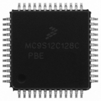
MC9S12C128CPBE Freescale Semiconductor, MC9S12C128CPBE Datasheet - Page 654

MC9S12C128CPBE
Manufacturer Part Number
MC9S12C128CPBE
Description
IC MCU 128K FLASH 25MHZ 52-LQFP
Manufacturer
Freescale Semiconductor
Series
HCS12r
Specifications of MC9S12C128CPBE
Core Processor
HCS12
Core Size
16-Bit
Speed
25MHz
Connectivity
CAN, EBI/EMI, SCI, SPI
Peripherals
POR, PWM, WDT
Number Of I /o
35
Program Memory Size
128KB (128K x 8)
Program Memory Type
FLASH
Ram Size
4K x 8
Voltage - Supply (vcc/vdd)
2.35 V ~ 5.5 V
Data Converters
A/D 8x10b
Oscillator Type
Internal
Operating Temperature
-40°C ~ 85°C
Package / Case
52-LQFP
Lead Free Status / RoHS Status
Lead free / RoHS Compliant
Eeprom Size
-
Available stocks
Company
Part Number
Manufacturer
Quantity
Price
Company:
Part Number:
MC9S12C128CPBE
Manufacturer:
Freescale Semiconductor
Quantity:
10 000
Company:
Part Number:
MC9S12C128CPBER
Manufacturer:
Freescale Semiconductor
Quantity:
10 000
- Current page: 654 of 690
- Download datasheet (4Mb)
Appendix A Electrical Characteristics
A.1.9
This section describes the characteristics of all I/O pins. All parameters are not always applicable, e.g. not
all pins feature pull up/down resistances.
1. Maximum leakage current occurs at maximum operating temperature. Current decreases by approximately one-half for each
2. Refer to
3. Parameter only applies in STOP or Pseudo STOP mode.
654
Conditions are 4.5< V
Num C
10
11
12
13
14
15
16
8 C to 12 C in the temper ature range from 50 C to 125 C .
1
2
3
4
5
6
7
8
9
P Input High Voltage
P Input Low Voltage
C Input Hysteresis
P
C
P
C
P
P
C
P
C
D Input Capacitance
P Port P, J Interrupt Input Pulse filtered
P Port P, J Interrupt Input Pulse passed
T Input High Voltage
T Input Low Voltage
T
Section A.1.4, “Current
Input Leakage Current (pins in high ohmic input mode)
Output High Voltage (pins in output mode)
Output High Voltage (pins in output mode)
Output Low Voltage (pins in output mode)
Output Low Voltage (pins in output mode)
Internal Pull Up Device Current,
tested at V
Internal Pull Up Device Current,
tested at V
Internal Pull Down Device Current,
tested at V
Internal Pull Down Device Current,
tested at V
Injection current
V
Partial Drive I OH = –2mA
Full Drive I
Partial Drive I
Full Drive I OL = +10mA
Single Pin limit
Total Device Limit. Sum of all injected currents
I/O Characteristics
in
= V
DD5
IL
IH
IH
IL
DDX
OH
or V
Max.
Max.
Min.
Min.
<5.5V Temperature from –40˚C to +140˚C, unless otherwise noted
OL
= –10mA
(2)
SS5
= +2mA
Injection”, for more details
Rating
MC9S12C-Family / MC9S12GC-Family
Table A-6. 5V I/O Characteristics
(3)
3
Rev 01.24
(1)
Symbol
V
t
t
I
I
V
V
I
I
V
V
PIGN
PVAL
I
I
V
V
PUH
PDH
V
V
PUL
PDL
C
ICS
ICP
HYS
I
OH
OH
in
OL
OL
IH
IH
IL
IL
in
V
V
0.65*V
V
DD5
DD5
SS5
–2.5
Min
–10
–25
10
10
—
—
—
—
—
—
—
—
—
– 0.8
– 0.8
- 0.3
DD5
Typ
250
—
—
—
—
—
—
—
—
—
—
—
—
—
—
—
—
—
7
Freescale Semiconductor
V
0.35*V
DD5
–130
Max
130
0.8
0.8
2.5
25
—
—
—
—
—
—
—
—
—
3
1
+ 0.3
DD5
Unit
mV
mΑ
µA
µA
µA
µA
µA
µs
µs
pf
V
V
V
V
V
V
V
V
Related parts for MC9S12C128CPBE
Image
Part Number
Description
Manufacturer
Datasheet
Request
R
Part Number:
Description:
Manufacturer:
Freescale Semiconductor, Inc
Datasheet:
Part Number:
Description:
Manufacturer:
Freescale Semiconductor, Inc
Datasheet:
Part Number:
Description:
Manufacturer:
Freescale Semiconductor, Inc
Datasheet:
Part Number:
Description:
Manufacturer:
Freescale Semiconductor, Inc
Datasheet:
Part Number:
Description:
Manufacturer:
Freescale Semiconductor, Inc
Datasheet:
Part Number:
Description:
Manufacturer:
Freescale Semiconductor, Inc
Datasheet:
Part Number:
Description:
Manufacturer:
Freescale Semiconductor, Inc
Datasheet:
Part Number:
Description:
Manufacturer:
Freescale Semiconductor, Inc
Datasheet:
Part Number:
Description:
Manufacturer:
Freescale Semiconductor, Inc
Datasheet:
Part Number:
Description:
Manufacturer:
Freescale Semiconductor, Inc
Datasheet:
Part Number:
Description:
Manufacturer:
Freescale Semiconductor, Inc
Datasheet:
Part Number:
Description:
Manufacturer:
Freescale Semiconductor, Inc
Datasheet:
Part Number:
Description:
Manufacturer:
Freescale Semiconductor, Inc
Datasheet:
Part Number:
Description:
Manufacturer:
Freescale Semiconductor, Inc
Datasheet:
Part Number:
Description:
Manufacturer:
Freescale Semiconductor, Inc
Datasheet:


