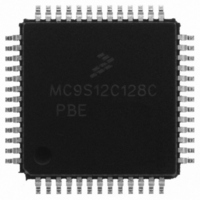
MC9S12C128CPBE Freescale Semiconductor, MC9S12C128CPBE Datasheet - Page 52

MC9S12C128CPBE
Manufacturer Part Number
MC9S12C128CPBE
Description
IC MCU 128K FLASH 25MHZ 52-LQFP
Manufacturer
Freescale Semiconductor
Series
HCS12r
Specifications of MC9S12C128CPBE
Core Processor
HCS12
Core Size
16-Bit
Speed
25MHz
Connectivity
CAN, EBI/EMI, SCI, SPI
Peripherals
POR, PWM, WDT
Number Of I /o
35
Program Memory Size
128KB (128K x 8)
Program Memory Type
FLASH
Ram Size
4K x 8
Voltage - Supply (vcc/vdd)
2.35 V ~ 5.5 V
Data Converters
A/D 8x10b
Oscillator Type
Internal
Operating Temperature
-40°C ~ 85°C
Package / Case
52-LQFP
Lead Free Status / RoHS Status
Lead free / RoHS Compliant
Eeprom Size
-
Available stocks
Company
Part Number
Manufacturer
Quantity
Price
Company:
Part Number:
MC9S12C128CPBE
Manufacturer:
Freescale Semiconductor
Quantity:
10 000
Company:
Part Number:
MC9S12C128CPBER
Manufacturer:
Freescale Semiconductor
Quantity:
10 000
- Current page: 52 of 690
- Download datasheet (4Mb)
Chapter 1 MC9S12C and MC9S12GC Device Overview (MC9S12C128)
1.3.4.9
PE6 is a general purpose input or output pin. It is used as a MCU operating mode select pin during reset.
The state of this pin is latched to the MODB bit at the rising edge of RESET. This pin is shared with the
instruction queue tracking signal IPIPE1. This pin is an input with a pull-down device which is only active
when RESET is low. PE[6] is not available in the 48- / 52-pin package versions.
1.3.4.10
PE5 is a general purpose input or output pin. It is used as a MCU operating mode select pin during reset.
The state of this pin is latched to the MODA bit at the rising edge of RESET. This pin is shared with the
instruction queue tracking signal IPIPE0. This pin is an input with a pull-down device which is only active
when RESET is low. This pin is not available in the 48- / 52-pin package versions.
1.3.4.11
ECLK is the output connection for the internal bus clock. It is used to demultiplex the address and data in
expanded modes and is used as a timing reference. ECLK frequency is equal to 1/2 the crystal frequency
out of reset. The ECLK pin is initially configured as ECLK output with stretch in all expanded modes. The
E clock output function depends upon the settings of the NECLK bit in the PEAR register, the IVIS bit in
the MODE register and the ESTR bit in the EBICTL register. All clocks, including the E clock, are halted
when the MCU is in stop mode. It is possible to configure the MCU to interface to slow external memory.
ECLK can be stretched for such accesses. Reference the MISC register (EXSTR[1:0] bits) for more
information. In normal expanded narrow mode, the E clock is available for use in external select decode
logic or as a constant speed clock for use in the external application system. Alternatively PE4 can be used
as a general purpose input or output pin.
1.3.4.12
In all modes this pin can be used as a general-purpose I/O and is an input with an active pull-up out of
reset. If the strobe function is required, it should be enabled by setting the LSTRE bit in the PEAR register.
This signal is used in write operations. Therefore external low byte writes will not be possible until this
function is enabled. This pin is also used as TAGLO in special expanded modes and is multiplexed with
the LSTRB function. This pin is not available in the 48- / 52-pin package versions.
52
PE6 / MODB / IPIPE1 — Port E I/O Pin 6
PE5 / MODA / IPIPE0 — Port E I/O Pin 5
PE4 / ECLK— Port E I/O Pin [4] / E-Clock Output
PE3 / LSTRB — Port E I/O Pin [3] / Low-Byte Strobe (LSTRB)
Figure 1-13. External Clock Connections (PE7 = 0)
MCU
MC9S12C-Family / MC9S12GC-Family
EXTAL
XTAL
Not Connected
Rev 01.24
CMOS Compatible
External Oscillator
(V
DDPLL
Level)
Freescale Semiconductor
Related parts for MC9S12C128CPBE
Image
Part Number
Description
Manufacturer
Datasheet
Request
R
Part Number:
Description:
Manufacturer:
Freescale Semiconductor, Inc
Datasheet:
Part Number:
Description:
Manufacturer:
Freescale Semiconductor, Inc
Datasheet:
Part Number:
Description:
Manufacturer:
Freescale Semiconductor, Inc
Datasheet:
Part Number:
Description:
Manufacturer:
Freescale Semiconductor, Inc
Datasheet:
Part Number:
Description:
Manufacturer:
Freescale Semiconductor, Inc
Datasheet:
Part Number:
Description:
Manufacturer:
Freescale Semiconductor, Inc
Datasheet:
Part Number:
Description:
Manufacturer:
Freescale Semiconductor, Inc
Datasheet:
Part Number:
Description:
Manufacturer:
Freescale Semiconductor, Inc
Datasheet:
Part Number:
Description:
Manufacturer:
Freescale Semiconductor, Inc
Datasheet:
Part Number:
Description:
Manufacturer:
Freescale Semiconductor, Inc
Datasheet:
Part Number:
Description:
Manufacturer:
Freescale Semiconductor, Inc
Datasheet:
Part Number:
Description:
Manufacturer:
Freescale Semiconductor, Inc
Datasheet:
Part Number:
Description:
Manufacturer:
Freescale Semiconductor, Inc
Datasheet:
Part Number:
Description:
Manufacturer:
Freescale Semiconductor, Inc
Datasheet:
Part Number:
Description:
Manufacturer:
Freescale Semiconductor, Inc
Datasheet:


