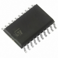
ST7FDALIF2M6 STMicroelectronics, ST7FDALIF2M6 Datasheet - Page 157

ST7FDALIF2M6
Manufacturer Part Number
ST7FDALIF2M6
Description
IC MCU 8BIT 8K 20-SOIC
Manufacturer
STMicroelectronics
Series
ST7r
Datasheet
1.ST7DALI-EVAL.pdf
(171 pages)
Specifications of ST7FDALIF2M6
Core Processor
ST7
Core Size
8-Bit
Speed
8MHz
Connectivity
DALI, SPI
Peripherals
LVD, POR, PWM, WDT
Number Of I /o
15
Program Memory Size
8KB (8K x 8)
Program Memory Type
FLASH
Eeprom Size
256 x 8
Ram Size
384 x 8
Voltage - Supply (vcc/vdd)
2.4 V ~ 5.5 V
Data Converters
A/D 7x10b
Oscillator Type
Internal
Operating Temperature
-40°C ~ 85°C
Package / Case
20-SOIC (7.5mm Width)
Processor Series
ST7DALI
Core
ST7
Data Bus Width
8 bit
Data Ram Size
384 B
Interface Type
DALI, SPI
Maximum Clock Frequency
8 MHz
Number Of Programmable I/os
15
Number Of Timers
4 bit
Operating Supply Voltage
2.4 V to 5.5 V
Maximum Operating Temperature
+ 85 C
Mounting Style
SMD/SMT
Development Tools By Supplier
ST7FLITE-SK/RAIS, ST7DALI-EVAL, ST7MDT10-DVP3, ST7MDT10-EMU3, STX-RLINK
Minimum Operating Temperature
- 40 C
On-chip Adc
8 bit
For Use With
497-5046 - KIT TOOL FOR ST7/UPSD/STR7 MCU
Lead Free Status / RoHS Status
Lead free / RoHS Compliant
Other names
497-2131-5
Available stocks
Company
Part Number
Manufacturer
Quantity
Price
Company:
Part Number:
ST7FDALIF2M6TR
Manufacturer:
NEC
Quantity:
670
ST7DALIF2
20.11.1
Table 91.
1. Data based on characterization results over the whole temperature range, not tested in production.
2. Please refer to the Application Note AN1830 for details of TE% vs Vin.
3. Refer to the offset variation in temperature below
4. Monotonicity guaranteed if V
5. For precise conversion results it is recommended to calibrate the amplifier at the following two points:
Amplifier output offset variation
The offset is quite sensitive to temperature variations. In order to ensure a good reliability in
measurements, the offset must be recalibrated periodically i.e. during power on or whenever
the device is reset depending on the customer application and during temperature variation.
The table below gives the typical offset variation over temperature:
Table 92.
V
V
V
V
Linearity
Gain factor
Vmax
Vmin
DD(AMP)
IN
OFFSET
STEP
- Offset at VINmin = 0V
- Gain at full scale (for example VIN=430 mV)
Symbol
-45
-12
Amplifier characteristics
Amplifier offset variation over temperature
Amplifier operating voltage
Amplifier input voltage
Amplifier output offset
voltage
Step size for monotonicity
Output Voltage Response
Amplified Analog input
Gain
Output Linearity Max Voltage V
Output Linearity Min Voltage
(5)
(3)
Typical offset variation (LSB)
Parameter
-20
IN
-7
increases or decreases in steps of min. 5 mV.
(2)
(4)
V
V
V
V
V
V
+25
DD
DD
DD
DD
DD
INmax
DD
-
Conditions
=3.6 V
=5 V
=5 V
=3.6 V
=5 V
=5 V
= 430 mV,
(1)
+90
+13
4.89
Min
3.6
3.5
0
0
Electrical characteristics
3.65
Typ
200
200
8
Linear
Max
3.94
350
500
5.5
Unit
LSB
°C
157/171
Unit
mV
mV
mV
mV
V
V


