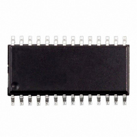
ST72C254G2M6 STMicroelectronics, ST72C254G2M6 Datasheet - Page 71

ST72C254G2M6
Manufacturer Part Number
ST72C254G2M6
Description
IC MCU 8BIT 8K FLASH SOIC-28
Manufacturer
STMicroelectronics
Series
ST7r
Datasheets
1.INDART-ST72C254.pdf
(3 pages)
2.ST72C104G1M6.pdf
(141 pages)
3.ST72C215G2M6.pdf
(140 pages)
Specifications of ST72C254G2M6
Core Processor
ST7
Core Size
8-Bit
Speed
16MHz
Connectivity
I²C, SPI
Peripherals
LVD, POR, PWM, WDT
Number Of I /o
22
Program Memory Size
8KB (8K x 8)
Program Memory Type
FLASH
Ram Size
256 x 8
Voltage - Supply (vcc/vdd)
3.2 V ~ 5.5 V
Data Converters
A/D 6x8b
Oscillator Type
Internal
Operating Temperature
-40°C ~ 85°C
Package / Case
28-SOIC (7.5mm Width)
Controller Family/series
ST7
No. Of I/o's
22
Ram Memory Size
256Byte
Cpu Speed
8MHz
No. Of Timers
2
Rohs Compliant
Yes
Processor Series
ST72C2x
Core
ST7
Data Bus Width
8 bit
Data Ram Size
256 B
Interface Type
I2C, SPI
Maximum Clock Frequency
16 MHz
Number Of Programmable I/os
22
Number Of Timers
3 bit
Operating Supply Voltage
3.2 V to 5.5 V
Maximum Operating Temperature
+ 85 C
Mounting Style
SMD/SMT
Development Tools By Supplier
ST7MDT1-DVP2/US
Minimum Operating Temperature
- 40 C
On-chip Adc
8 bit
Lead Free Status / RoHS Status
Lead free / RoHS Compliant
Eeprom Size
-
Lead Free Status / Rohs Status
In Transition
Available stocks
Company
Part Number
Manufacturer
Quantity
Price
Part Number:
ST72C254G2M6
Manufacturer:
ST
Quantity:
20 000
SERIAL PERIPHERAL INTERFACE (Cont’d)
STATUS REGISTER (SR)
Read Only
Reset Value: 0000 0000 (00h)
Bit 7 = SPIF Serial Peripheral data transfer flag.
This bit is set by hardware when a transfer has
been completed. An interrupt is generated if
SPIE=1 in the CR register. It is cleared by a soft-
ware sequence (an access to the SR register fol-
lowed by a read or write to the DR register).
0: Data transfer is in progress or has been ap-
1: Data transfer between the device and an exter-
Note: While the SPIF bit is set, all writes to the DR
register are inhibited.
Bit 6 = WCOL Write Collision status.
This bit is set by hardware when a write to the DR
register is done during a transmit sequence. It is
cleared by a software sequence (see
0: No write collision occurred
1: A write collision has been detected
Bit 5 = Unused.
Bit 4 = MODF Mode Fault flag.
This bit is set by hardware when the SS pin is
pulled low in master mode (see
"Master Mode Fault" on page
can be generated if SPIE=1 in the CR register.
This bit is cleared by a software sequence (An ac-
cess to the SR register while MODF=1 followed by
a write to the CR register).
0: No master mode fault detected
1: A fault in master mode has been detected
Bits 3-0 = Unused.
SPIF
proved by a clearing sequence.
nal device has been completed.
7
WCOL
-
MODF
70). An SPI interrupt
-
Section 12.3.4.5
-
Figure
-
41).
0
-
ST72104G, ST72215G, ST72216G, ST72254G
DATA I/O REGISTER (DR)
Read/Write
Reset Value: Undefined
The DR register is used to transmit and receive
data on the serial bus. In the master device only a
write to this register will initiate transmission/re-
ception of another byte.
Notes: During the last clock cycle the SPIF bit is
set, a copy of the received data byte in the shift
register is moved to a buffer. When the user reads
the serial peripheral data I/O register, the buffer is
actually being read.
Warning:
A write to the DR register places data directly into
the shift register for transmission.
A write to the the DR register returns the value lo-
cated in the buffer and not the contents of the shift
register (See
D7
7
D6
Figure 38
D5
D4
).
D3
D2
D1
71/140
D0
0


