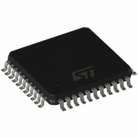
ST72F561J4T6 STMicroelectronics, ST72F561J4T6 Datasheet - Page 190

ST72F561J4T6
Manufacturer Part Number
ST72F561J4T6
Description
IC MCU 8BIT 16K FLASH 44-LQFP
Manufacturer
STMicroelectronics
Series
ST7r
Datasheet
1.ST72F561K6T6.pdf
(265 pages)
Specifications of ST72F561J4T6
Core Processor
ST7
Core Size
8-Bit
Speed
8MHz
Connectivity
CAN, LINSCI, SPI
Peripherals
LVD, POR, PWM, WDT
Number Of I /o
32
Program Memory Size
16KB (16K x 8)
Program Memory Type
FLASH
Ram Size
1K x 8
Voltage - Supply (vcc/vdd)
3.8 V ~ 5.5 V
Data Converters
A/D 16x10b
Oscillator Type
External
Operating Temperature
-40°C ~ 85°C
Package / Case
44-LQFP
Processor Series
ST72F5x
Core
ST7
Data Bus Width
8 bit
Data Ram Size
1 KB
Interface Type
CAN, SCI, SPI
Maximum Clock Frequency
8 MHz
Number Of Programmable I/os
48
Number Of Timers
3
Maximum Operating Temperature
+ 85 C
Mounting Style
SMD/SMT
Development Tools By Supplier
STX-RLINK
Minimum Operating Temperature
- 40 C
On-chip Adc
10 bit, 16 Channel
For Use With
497-8374 - BOARD DEVELOPMENT FOR ST72F561
Lead Free Status / RoHS Status
Lead free / RoHS Compliant
Eeprom Size
-
Lead Free Status / Rohs Status
Details
Available stocks
Company
Part Number
Manufacturer
Quantity
Price
Company:
Part Number:
ST72F561J4T6
Manufacturer:
COILCRAFT
Quantity:
4 000
Company:
Part Number:
ST72F561J4T6
Manufacturer:
STMicroelectronics
Quantity:
10 000
- Current page: 190 of 265
- Download datasheet (10Mb)
ST72561
beCAN CONTROLLER (Cont’d)
Side-effect of Workround 1
Because the while loop lasts 10 CPU cycles, at
high baud rate, it is possible to miss a dominant
state on the bus if it lasts just one CAN bit time and
the bus speed is high enough (see
Table 29. While Loop Timing
If this happens, we will continue waiting in the
while loop instead of releasing the FIFO immedi-
ately. The workaround is still valid because we will
not release the FIFO during the critical period. But
the application may lose additional time waiting in
the while loop as we are no longer able to guaran-
tee a maximum of 6 CAN bit times spent in the
workaround.
In this particular case the time the application can
spend in the workaround may increase up to a full
CAN frame, depending of the frame contents. This
Figure 113. Reception at Maximum CAN Baud Rate
190/265
Sampling of Rx pin
8 MHz
4 MHz
CAN Bus signal
f
f
CPU
CPU
While loop
Software
10/f
1.25 µs
timing:
2.5 µs
CPU
R
R
Minimum baud rate for
R
possible missed
dominant bit
800 Kbaud
400 Kbaud
Table
R
f
CPU
D
/10
R
1).
R
R
R
D
case is very rare but happens when a specific se-
quence is present on in the CAN frame.
The example in
imum CAN baud rate: In this case t
and the sampling time is 10/f
If the application is using the maximum baud rate
and the possible delay caused by the workaround
is not acceptable, there is another workaround
which reduces the Rx pin sampling time.
Workaround 2 (see
FMP = 2 and the CAN cell is receiving, if not the
FIFO can be released immediately. If yes, the pro-
gram goes through a sequence of test instructions
on the RX pin that last longer than the time be-
tween the acknowledge dominant bit and the criti-
cal time slot. If the Rx pin is in recessive state for
more than 8 CAN bit times, it means we are now
after the acknowledge and the critical slot. If a
dominant bit is read on the bus, we can release the
FIFO immediately. This workaround has to be writ-
ten in assembly language to avoid the compiler
optimizing the test sequence.
The implementation shown here is for the CAN
bus maximum speed (1 Mbaud @ 8 MHz CPU
clock).
R
R
R
R
D
Figure 20
R
R
Figure
R
shows reception at max-
R
CPU
21) first tests that
D
.
R
R
CAN
R
is 8/f
R
D
CPU
Related parts for ST72F561J4T6
Image
Part Number
Description
Manufacturer
Datasheet
Request
R

Part Number:
Description:
STMicroelectronics [RIPPLE-CARRY BINARY COUNTER/DIVIDERS]
Manufacturer:
STMicroelectronics
Datasheet:

Part Number:
Description:
STMicroelectronics [LIQUID-CRYSTAL DISPLAY DRIVERS]
Manufacturer:
STMicroelectronics
Datasheet:

Part Number:
Description:
BOARD EVAL FOR MEMS SENSORS
Manufacturer:
STMicroelectronics
Datasheet:

Part Number:
Description:
NPN TRANSISTOR POWER MODULE
Manufacturer:
STMicroelectronics
Datasheet:

Part Number:
Description:
TURBOSWITCH ULTRA-FAST HIGH VOLTAGE DIODE
Manufacturer:
STMicroelectronics
Datasheet:

Part Number:
Description:
Manufacturer:
STMicroelectronics
Datasheet:

Part Number:
Description:
DIODE / SCR MODULE
Manufacturer:
STMicroelectronics
Datasheet:

Part Number:
Description:
DIODE / SCR MODULE
Manufacturer:
STMicroelectronics
Datasheet:

Part Number:
Description:
Search -----> STE16N100
Manufacturer:
STMicroelectronics
Datasheet:

Part Number:
Description:
Search ---> STE53NA50
Manufacturer:
STMicroelectronics
Datasheet:

Part Number:
Description:
NPN Transistor Power Module
Manufacturer:
STMicroelectronics
Datasheet:

Part Number:
Description:
DIODE / SCR MODULE
Manufacturer:
STMicroelectronics
Datasheet:


