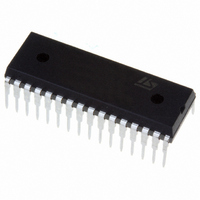
ST72F262G2B5 STMicroelectronics, ST72F262G2B5 Datasheet - Page 99

ST72F262G2B5
Manufacturer Part Number
ST72F262G2B5
Description
IC MCU 8BIT 8K FLASH 32-SDIP
Manufacturer
STMicroelectronics
Series
ST7r
Datasheet
1.STEVAL-ISQ002V1.pdf
(172 pages)
Specifications of ST72F262G2B5
Core Processor
ST7
Core Size
8-Bit
Speed
16MHz
Connectivity
SPI
Peripherals
LVD, POR, PWM, WDT
Number Of I /o
22
Program Memory Size
8KB (8K x 8)
Program Memory Type
FLASH
Ram Size
256 x 8
Voltage - Supply (vcc/vdd)
2.7 V ~ 5.5 V
Data Converters
A/D 6x10b
Oscillator Type
Internal
Operating Temperature
-10°C ~ 85°C
Package / Case
32-SDIP (0.400", 10.16mm)
Processor Series
ST72F2x
Core
ST7
Data Bus Width
8 bit
Data Ram Size
256 B
Interface Type
I2C, SCI, SPI
Maximum Clock Frequency
8 MHz
Number Of Programmable I/os
22
Number Of Timers
16 bit
Maximum Operating Temperature
+ 85 C
Mounting Style
Through Hole
Development Tools By Supplier
ST7F264-IND/USB, ST72F34X-SK/RAIS, ST7MDT10-DVP3, ST7MDT10-EMU3, STX-RLINK
Minimum Operating Temperature
- 40 C
On-chip Adc
8 bit
Lead Free Status / RoHS Status
Lead free / RoHS Compliant
Eeprom Size
-
Lead Free Status / Rohs Status
Details
Available stocks
Company
Part Number
Manufacturer
Quantity
Price
Company:
Part Number:
ST72F262G2B5
Manufacturer:
TAIYO
Quantity:
8 122
SERIAL COMMUNICATIONS INTERFACE (Cont’d)
CONTROL REGISTER 2 (SCICR2)
Read/Write
Reset Value: 0000 0000 (00h)
Bit 7 = TIE Transmitter interrupt enable.
This bit is set and cleared by software.
0: Interrupt is inhibited
1: An SCI interrupt is generated whenever
Bit 6 = TCIE Transmission complete interrupt ena-
ble
This bit is set and cleared by software.
0: Interrupt is inhibited
1: An SCI interrupt is generated whenever TC=1 in
Bit 5 = RIE Receiver interrupt enable.
This bit is set and cleared by software.
0: Interrupt is inhibited
1: An SCI interrupt is generated whenever OR=1
Bit 4 = ILIE Idle line interrupt enable.
This bit is set and cleared by software.
0: Interrupt is inhibited
1: An SCI interrupt is generated whenever IDLE=1
Bit 3 = TE Transmitter enable.
This bit enables the transmitter. It is set and
cleared by software.
0: Transmitter is disabled
1: Transmitter is enabled
TIE
TDRE=1 in the SCISR register
the SCISR register
or RDRF=1 in the SCISR register
in the SCISR register.
7
TCIE
RIE
ILIE
TE
RE
RWU
SBK
0
Notes:
– During transmission, a “0” pulse on the TE bit
– When TE is set there is a 1 bit-time delay before
Caution: The TDO pin is free for general purpose
I/O only when the TE and RE bits are both cleared
(or if TE is never set).
Bit 2 = RE Receiver enable.
This bit enables the receiver. It is set and cleared
by software.
0: Receiver is disabled
1: Receiver is enabled and begins searching for a
Bit 1 = RWU Receiver wake-up.
This bit determines if the SCI is in mute mode or
not. It is set and cleared by software and can be
cleared by hardware when a wake-up sequence is
recognized.
0: Receiver in Active mode
1: Receiver in Mute mode
Note: Before selecting Mute mode (setting the
RWU bit), the SCI must receive some data first,
otherwise it cannot function in Mute mode with
wakeup by idle line detection.
Bit 0 = SBK Send break.
This bit set is used to send break characters. It is
set and cleared by software.
0: No break character is transmitted
1: Break characters are transmitted
Note: If the SBK bit is set to “1” and then to “0”, the
transmitter will send a BREAK word at the end of
the current word.
(“0” followed by “1”) sends a preamble (idle line)
after the current word.
the transmission starts.
start bit
ST72260Gx, ST72262Gx, ST72264Gx
99/172


