ST72F262G2B5 STMicroelectronics, ST72F262G2B5 Datasheet - Page 144

ST72F262G2B5
Manufacturer Part Number
ST72F262G2B5
Description
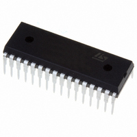
IC MCU 8BIT 8K FLASH 32-SDIP
Manufacturer
STMicroelectronics
Series
ST7r
Datasheet
1.STEVAL-ISQ002V1.pdf
(172 pages)
Specifications of ST72F262G2B5
Core Processor
ST7
Core Size
8-Bit
Speed
16MHz
Connectivity
SPI
Peripherals
LVD, POR, PWM, WDT
Number Of I /o
22
Program Memory Size
8KB (8K x 8)
Program Memory Type
FLASH
Ram Size
256 x 8
Voltage - Supply (vcc/vdd)
2.7 V ~ 5.5 V
Data Converters
A/D 6x10b
Oscillator Type
Internal
Operating Temperature
-10°C ~ 85°C
Package / Case
32-SDIP (0.400", 10.16mm)
Processor Series
ST72F2x
Core
ST7
Data Bus Width
8 bit
Data Ram Size
256 B
Interface Type
I2C, SCI, SPI
Maximum Clock Frequency
8 MHz
Number Of Programmable I/os
22
Number Of Timers
16 bit
Maximum Operating Temperature
+ 85 C
Mounting Style
Through Hole
Development Tools By Supplier
ST7F264-IND/USB, ST72F34X-SK/RAIS, ST7MDT10-DVP3, ST7MDT10-EMU3, STX-RLINK
Minimum Operating Temperature
- 40 C
On-chip Adc
8 bit
Lead Free Status / RoHS Status
Lead free / RoHS Compliant
Eeprom Size
-
Lead Free Status / Rohs Status
Details
Available stocks
Company
Part Number
Manufacturer
Quantity
Price
Company:
Part Number:
ST72F262G2B5
Manufacturer:
TAIYO
Quantity:
8 122
ST72260Gx, ST72262Gx, ST72264Gx
13.8 I/O PORT PIN CHARACTERISTICS
13.8.1 General Characteristics
T
Notes:
1. Data based on characterization results, not tested in production.
2. I
respected, the injection current must be limited externally to the I
while a negative injection is induced by V
corresponding V
Caution: Negative current injection not allowed on Flash device pins PB0 and PB1.
3. Configuration not recommended, all unused pins must be kept at a fixed voltage: using the output mode of the I/O for
example and leaving the I/O unconnected on the board or an external pull-up or pull-down resistor (see
based on design simulation and/or technology characteristics, not tested in production.
4. The R
scribed in
5. To generate an external interrupt, a minimum pulse width has to be applied on an I/O port pin configured as an external
interrupt source.
Figure 76. Two typical Applications with unused I/O Pin configured as input
144/172
ΣI
I
A
Symbol
INJ(PIN)
t
t
INJ(PIN)
t
f(IO)out
r(IO)out
w(IT)in
INJ(PIN)
V
R
= -40 to +85°C unless otherwise specified
C
V
V
I
I
hys
PU
S
IH
L
IO
IL
Note: I/O can be left unconnected if it is configured as output (0 or 1) by the software. This has the advantage of greater EMC
robustness and lower cost.
2)
PU
2)
Figure
must never be exceeded. This is implicitly insured if V
Input low level voltage
Input high level voltage
Schmitt trigger voltage hysteresis
Injected current on Flash device
pins PB0 and PB1
Injected Current on other I/O pins
Total injected current (sum of all I/O
and control pins)
Input leakage current
Static current consumption
Weak pull-up equivalent resistor
I/O pin capacitance
Output high to low level fall time
Output low to high level rise time
External interrupt pulse time
pull-up equivalent resistor is based on a resistive transistor (corresponding I
IN
77).
maximum must always be respected.
V
DD
Parameter
10kΩ
UNUSED I/O PORT
1)
1)
5)
IN
ST7XXX
<V
4)
1)
SS
1)
1)
. For true open-drain pads, there is no positive injection current, and the
V
V
Floating input mode
V
C
Between 10% and 90%
DD
SS
IN
L
=50pF
=
≤
=5V
V
V
SS
IN
Conditions
≤
V
DD
V
V
INJ(PIN)
DD
DD
IN
=5V
=3V
maximum is respected. If V
3)
value. A positive injection is induced by V
10kΩ
0.7xV
V
170
ss
Min
50
1
- 0.3
UNUSED I/O PORT
1)
DD
ST7XXX
PU
Typ
400
400
190
85
25
25
5
current characteristics de-
IN
maximum cannot be
V
0.3xV
DD
230
Max
±25
250
+4
±4
±1
Figure
+ 0.3
1)
DD
76). Data
IN
t
Unit
mV
mA
CPU
µA
kΩ
pF
ns
V
>V
DD


