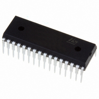
ST72F262G2B5 STMicroelectronics, ST72F262G2B5 Datasheet - Page 38

ST72F262G2B5
Manufacturer Part Number
ST72F262G2B5
Description
IC MCU 8BIT 8K FLASH 32-SDIP
Manufacturer
STMicroelectronics
Series
ST7r
Datasheet
1.STEVAL-ISQ002V1.pdf
(172 pages)
Specifications of ST72F262G2B5
Core Processor
ST7
Core Size
8-Bit
Speed
16MHz
Connectivity
SPI
Peripherals
LVD, POR, PWM, WDT
Number Of I /o
22
Program Memory Size
8KB (8K x 8)
Program Memory Type
FLASH
Ram Size
256 x 8
Voltage - Supply (vcc/vdd)
2.7 V ~ 5.5 V
Data Converters
A/D 6x10b
Oscillator Type
Internal
Operating Temperature
-10°C ~ 85°C
Package / Case
32-SDIP (0.400", 10.16mm)
Processor Series
ST72F2x
Core
ST7
Data Bus Width
8 bit
Data Ram Size
256 B
Interface Type
I2C, SCI, SPI
Maximum Clock Frequency
8 MHz
Number Of Programmable I/os
22
Number Of Timers
16 bit
Maximum Operating Temperature
+ 85 C
Mounting Style
Through Hole
Development Tools By Supplier
ST7F264-IND/USB, ST72F34X-SK/RAIS, ST7MDT10-DVP3, ST7MDT10-EMU3, STX-RLINK
Minimum Operating Temperature
- 40 C
On-chip Adc
8 bit
Lead Free Status / RoHS Status
Lead free / RoHS Compliant
Eeprom Size
-
Lead Free Status / Rohs Status
Details
Available stocks
Company
Part Number
Manufacturer
Quantity
Price
Company:
Part Number:
ST72F262G2B5
Manufacturer:
TAIYO
Quantity:
8 122
ST72260Gx, ST72262Gx, ST72264Gx
9 I/O PORTS
9.1 INTRODUCTION
The I/O ports allow data transfer. An I/O port can
contain up to 8 pins. Each pin can be programmed
independently either as a digital input or digital
output. In addition, specific pins may have several
other functions. These functions can include exter-
nal interrupt, alternate signal input/output for on-
chip peripherals or analog input.
9.2 FUNCTIONAL DESCRIPTION
A Data Register (DR) and a Data Direction Regis-
ter (DDR) are always associated with each port.
The Option Register (OR), which allows input/out-
put options, may or may not be implemented. The
following description takes into account the OR
register. Refer to the Port Configuration table for
device specific information.
An I/O pin is programmed using the corresponding
bits in the DDR, DR and OR registers: bit x corre-
sponding to pin x of the port.
Figure 27
9.2.1 Input Modes
Clearing the DDRx bit selects input mode. In this
mode, reading its DR bit returns the digital value
from that I/O pin.
If an OR bit is available, different input modes can
be configured by software: floating or pull-up. Re-
fer to I/O Port Implementation section for configu-
ration.
Notes:
1. Writing to the DR modifies the latch value but
does not change the state of the input pin.
2. Do not use read/modify/write instructions
(BSET/BRES) to modify the DR register.
External Interrupt Function
Depending on the device, setting the ORx bit while
in input mode can configure an I/O as an input with
interrupt. In this configuration, a signal edge or lev-
el input on the I/O generates an interrupt request
via the corresponding interrupt vector (eix).
Falling or rising edge sensitivity is programmed in-
dependently for each interrupt vector. The Exter-
nal Interrupt Control Register (EICR) or the Miscel-
laneous Register controls this sensitivity, depend-
ing on the device.
A device may have up to 7 external interrupts.
Several pins may be tied to one external interrupt
vector. Refer to Pin Description to see which ports
have external interrupts.
38/172
shows the generic I/O block diagram.
If several I/O interrupt pins on the same interrupt
vector are selected simultaneously, they are logi-
cally combined. For this reason if one of the inter-
rupt pins is tied low, it may mask the others.
External interrupts are hardware interrupts. Fetch-
ing the corresponding interrupt vector automatical-
ly clears the request latch. Modifying the sensitivity
bits will clear any pending interrupts.
9.2.2 Output Modes
Setting the DDRx bit selects output mode. Writing
to the DR bits applies a digital value to the I/O
through the latch. Reading the DR bits returns the
previously stored value.
If an OR bit is available, different output modes
can be selected by software: push-pull or open-
drain. Refer to I/O Port Implementation section for
configuration.
DR Value and Output Pin Status
9.2.3 Alternate Functions
Many ST7s I/Os have one or more alternate func-
tions. These may include output signals from, or
input signals to, on-chip peripherals. The Device
Pin Description table describes which peripheral
signals can be input/output to which ports.
A signal coming from an on-chip peripheral can be
output on an I/O. To do this, enable the on-chip
peripheral as an output (enable bit in the peripher-
al’s control register). The peripheral configures the
I/O as an output and takes priority over standard I/
O programming. The I/O’s state is readable by ad-
dressing the corresponding I/O data register.
Configuring an I/O as floating enables alternate
function input. It is not recommended to configure
an I/O as pull-up as this will increase current con-
sumption. Before using an I/O as an alternate in-
put, configure it without interrupt. Otherwise spuri-
ous interrupts can occur.
Configure an I/O as input floating for an on-chip
peripheral signal which can be input and output.
Caution:
I/Os which can be configured as both an analog
and digital alternate function need special atten-
tion. The user must control the peripherals so that
the signals do not arrive at the same time on the
same pin. If an external clock is used, only the
clock alternate function should be employed on
that I/O pin and not the other alternate function.
DR
0
1
Push-Pull
V
V
OH
OL
Open-Drain
Floating
V
OL


