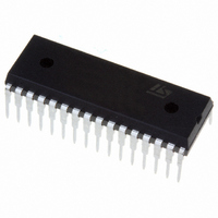
ST72F262G2B5 STMicroelectronics, ST72F262G2B5 Datasheet - Page 47

ST72F262G2B5
Manufacturer Part Number
ST72F262G2B5
Description
IC MCU 8BIT 8K FLASH 32-SDIP
Manufacturer
STMicroelectronics
Series
ST7r
Datasheet
1.STEVAL-ISQ002V1.pdf
(172 pages)
Specifications of ST72F262G2B5
Core Processor
ST7
Core Size
8-Bit
Speed
16MHz
Connectivity
SPI
Peripherals
LVD, POR, PWM, WDT
Number Of I /o
22
Program Memory Size
8KB (8K x 8)
Program Memory Type
FLASH
Ram Size
256 x 8
Voltage - Supply (vcc/vdd)
2.7 V ~ 5.5 V
Data Converters
A/D 6x10b
Oscillator Type
Internal
Operating Temperature
-10°C ~ 85°C
Package / Case
32-SDIP (0.400", 10.16mm)
Processor Series
ST72F2x
Core
ST7
Data Bus Width
8 bit
Data Ram Size
256 B
Interface Type
I2C, SCI, SPI
Maximum Clock Frequency
8 MHz
Number Of Programmable I/os
22
Number Of Timers
16 bit
Maximum Operating Temperature
+ 85 C
Mounting Style
Through Hole
Development Tools By Supplier
ST7F264-IND/USB, ST72F34X-SK/RAIS, ST7MDT10-DVP3, ST7MDT10-EMU3, STX-RLINK
Minimum Operating Temperature
- 40 C
On-chip Adc
8 bit
Lead Free Status / RoHS Status
Lead free / RoHS Compliant
Eeprom Size
-
Lead Free Status / Rohs Status
Details
Available stocks
Company
Part Number
Manufacturer
Quantity
Price
Company:
Part Number:
ST72F262G2B5
Manufacturer:
TAIYO
Quantity:
8 122
MISCELLANEOUS REGISTERS (Cont’d)
MISCELLANEOUS REGISTER 2 (MISCR2)
Read/Write
Reset Value: 0000 0000 (00h)
Caution: This register has been provided for com-
patibility with the ST72254 family only. The same
bits are available in the SPICSR register. New ap-
plications must use the SPICSR register. Do not
use both registers, this will cause the SPI to mal-
function.
Bits 7:4 = Reserved always read as 0
Bits 3 = MOD SPI Master Output Disable
This bit is set and cleared by software. When set, it
disables the SPI Master (MOSI) output signal.
0: SPI Master Output enabled.
1: SPI Master Output disabled.
Bit 2 = SOD SPI Slave Output Disable
This bit is set and cleared by software. When set it
disable the SPI Slave (MISO) output signal.
0: SPI Slave Output enabled.
1: SPI Slave Output disabled.
Bit 1 = SSM SS mode selection
This bit is set and cleared by software.
0: Normal mode - the level of the SPI SS signal is
1: I/O mode, the level of the SPI SS signal is read
Bit 0 = SSI SS internal mode
This bit replaces the SS pin of the SPI when the
SSM bit is set to 1. (see SPI description). It is set
and cleared by software.
Table 11. Miscellaneous Register Map and Reset Values
Address
input from the external SS pin.
from the SSI bit.
7
0
(Hex.)
0020h
0040h
0
MISCR1
Reset Value
MISCR2
Reset Value
Register
0
Label
0
MOD SOD SSM
IS11
7
0
0
IS10
6
0
0
SSI
0
MCO
5
0
0
IS01
4
0
0
ST72260Gx, ST72262Gx, ST72264Gx
MOD
IS00
3
0
0
SOD
CP1
2
0
0
SSM
CP0
1
0
0
SMS
SSI
47/172
0
0
0


