ST7FLI49MK1T6 STMicroelectronics, ST7FLI49MK1T6 Datasheet - Page 99
ST7FLI49MK1T6
Manufacturer Part Number
ST7FLI49MK1T6
Description
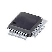
MCU 8BIT SGL VOLT FLASH 32-LQFP
Manufacturer
STMicroelectronics
Series
ST7r
Datasheet
1.ST7FLI49MK1T6TR.pdf
(187 pages)
Specifications of ST7FLI49MK1T6
Core Processor
ST7
Core Size
8-Bit
Speed
8MHz
Connectivity
I²C
Peripherals
LVD, POR, PWM, WDT
Number Of I /o
24
Program Memory Size
4KB (4K x 8)
Program Memory Type
FLASH
Eeprom Size
128 x 8
Ram Size
384 x 8
Voltage - Supply (vcc/vdd)
2.4 V ~ 5.5 V
Data Converters
A/D 10x10b
Oscillator Type
Internal
Operating Temperature
-40°C ~ 85°C
Package / Case
32-LQFP
Processor Series
ST7FLI4x
Core
ST7
Data Bus Width
8 bit
Data Ram Size
384 B
Interface Type
I2C
Maximum Clock Frequency
8 MHz
Number Of Programmable I/os
24
Number Of Timers
5
Maximum Operating Temperature
+ 125 C
Mounting Style
SMD/SMT
Minimum Operating Temperature
- 40 C
On-chip Adc
10 bit, 10 Channel
Lead Free Status / RoHS Status
Lead free / RoHS Compliant
Available stocks
Company
Part Number
Manufacturer
Quantity
Price
Company:

Part Number:
ST7FLI49MK1T6
Manufacturer:
st
Quantity:
456
Company:
Part Number:
ST7FLI49MK1T6
Manufacturer:
STMicroelectronics
Quantity:
10 000
Part Number:
ST7FLI49MK1T6
Manufacturer:
ST
Quantity:
20 000
Company:
Part Number:
ST7FLI49MK1T6TR
Manufacturer:
STMicroelectronics
Quantity:
10 000


ST7LITE49M
Note:
Note:
1
2
1
2
3
Bit 1= TRAN2 Transfer enable2 bit
DCR2/3 transfer will be controlled using this bit if ENCNTR2 bit is set.
This bit must not be reset by software
Bit 0 = TRAN1 Transfer enable 1 bit
DCR0,1 transfers are always controlled using this bit.
DCR2/3 transfer will be controlled using this bit if ENCNTR2 is reset.
This bit must not be reset by software
Autoreload register 2 (ATR2H)
Reset value: 0000 0000 (00h)
Autoreload register (ATR2L)
Reset value: 0000 0000 (00h)
Bits 11:0 = ATR2[11:0] Autoreload register 2
This is a 12-bit register which is written by software. The ATR2 register value is
automatically loaded into the upcounter CNTR2 when an overflow of CNTR2 occurs. The
register value is used to set the PWM2/PWM3 frequency when ENCNTR2 is set.
ATR7
This bit is read/write by software, cleared by hardware after each completed transfer
and set by hardware after reset. It controls the transfers on CNTR2.
It allows the value of the Preload DCRx registers to be transferred to the Active DCRx
registers after the next overflow event.
The OPx bits are transferred to the shadow OPx bits in the same way.
This bit is read/write by software, cleared by hardware after each completed transfer
and set by hardware after reset. It controls the transfers on CNTR1. It allows the value
of the Preload DCRx registers to be transferred to the Active DCRx registers after the
next overflow event.
The OPx bits are transferred to the shadow OPx bits in the same way.
15
0
7
ATR6
0
ATR5
0
Doc ID 13562 Rev 3
ATR4
0
Read/write
Read/write
ATR11
ATR3
ATR10
ATR2
On-chip peripherals
ATR9
ATR1
ATR0
ATR8
0
8
99/188
Related parts for ST7FLI49MK1T6
Image
Part Number
Description
Manufacturer
Datasheet
Request
R

Part Number:
Description:
BOARD DAUGHTER 32LQFP ST7FLITE4
Manufacturer:
STMicroelectronics
Datasheet:
Part Number:
Description:
STMicroelectronics [RIPPLE-CARRY BINARY COUNTER/DIVIDERS]
Manufacturer:
STMicroelectronics
Datasheet:
Part Number:
Description:
STMicroelectronics [LIQUID-CRYSTAL DISPLAY DRIVERS]
Manufacturer:
STMicroelectronics
Datasheet:

Part Number:
Description:
BOARD EVAL FOR MEMS SENSORS
Manufacturer:
STMicroelectronics
Datasheet:
Part Number:
Description:
NPN TRANSISTOR POWER MODULE
Manufacturer:
STMicroelectronics
Datasheet:
Part Number:
Description:
TURBOSWITCH ULTRA-FAST HIGH VOLTAGE DIODE
Manufacturer:
STMicroelectronics
Datasheet:
Part Number:
Description:
Manufacturer:
STMicroelectronics
Datasheet:
Part Number:
Description:
DIODE / SCR MODULE
Manufacturer:
STMicroelectronics
Datasheet:
Part Number:
Description:
DIODE / SCR MODULE
Manufacturer:
STMicroelectronics
Datasheet:
Part Number:
Description:
Search -----> STE16N100
Manufacturer:
STMicroelectronics
Datasheet:
Part Number:
Description:
Search ---> STE53NA50
Manufacturer:
STMicroelectronics
Datasheet:
Part Number:
Description:
NPN Transistor Power Module
Manufacturer:
STMicroelectronics
Datasheet: