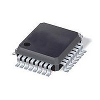
ST7FLI49MK1T6 STMicroelectronics, ST7FLI49MK1T6 Datasheet - Page 21

ST7FLI49MK1T6
Manufacturer Part Number
ST7FLI49MK1T6
Description
MCU 8BIT SGL VOLT FLASH 32-LQFP
Manufacturer
STMicroelectronics
Series
ST7r
Datasheet
1.ST7FLI49MK1T6TR.pdf
(187 pages)
Specifications of ST7FLI49MK1T6
Core Processor
ST7
Core Size
8-Bit
Speed
8MHz
Connectivity
I²C
Peripherals
LVD, POR, PWM, WDT
Number Of I /o
24
Program Memory Size
4KB (4K x 8)
Program Memory Type
FLASH
Eeprom Size
128 x 8
Ram Size
384 x 8
Voltage - Supply (vcc/vdd)
2.4 V ~ 5.5 V
Data Converters
A/D 10x10b
Oscillator Type
Internal
Operating Temperature
-40°C ~ 85°C
Package / Case
32-LQFP
Processor Series
ST7FLI4x
Core
ST7
Data Bus Width
8 bit
Data Ram Size
384 B
Interface Type
I2C
Maximum Clock Frequency
8 MHz
Number Of Programmable I/os
24
Number Of Timers
5
Maximum Operating Temperature
+ 125 C
Mounting Style
SMD/SMT
Minimum Operating Temperature
- 40 C
On-chip Adc
10 bit, 10 Channel
Lead Free Status / RoHS Status
Lead free / RoHS Compliant
Available stocks
Company
Part Number
Manufacturer
Quantity
Price
Company:
Part Number:
ST7FLI49MK1T6
Manufacturer:
st
Quantity:
456
Company:
Part Number:
ST7FLI49MK1T6
Manufacturer:
STMicroelectronics
Quantity:
10 000
Part Number:
ST7FLI49MK1T6
Manufacturer:
ST
Quantity:
20 000
Company:
Part Number:
ST7FLI49MK1T6TR
Manufacturer:
STMicroelectronics
Quantity:
10 000
ST7LITE49M
4.3.2
4.4
Note:
Caution:
1
2
3
4
Depending on the ICP Driver code downloaded in RAM, Flash memory programming can
be fully customized (number of bytes to program, program locations, or selection of the
serial communication interface for downloading).
In-application programming (IAP)
This mode uses an IAP Driver program previously programmed in Sector 0 by the user (in
ICP mode).
This mode is fully controlled by user software. This allows it to be adapted to the user
application, (user-defined strategy for entering programming mode, choice of
communications protocol used to fetch the data to be stored etc.)
IAP mode can be used to program any memory areas except Sector 0, which is Write/Erase
protected to allow recovery in case errors occur during the programming operation.
ICC interface
ICP needs a minimum of 4 and up to 6 pins to be connected to the programming tool. These
pins are:
●
●
●
●
●
●
If the ICCCLK or ICCDATA pins are only used as outputs in the application, no signal
isolation is necessary. As soon as the Programming Tool is plugged to the board, even if an
ICC session is not in progress, the ICCCLK and ICCDATA pins are not available for the
application. If they are used as inputs by the application, isolation such as a serial resistor
has to be implemented in case another device forces the signal. Refer to the Programming
Tool documentation for recommended resistor values.
During the ICP session, the programming tool must control the RESET pin. This can lead to
conflicts between the programming tool and the application reset circuit if it drives more than
5 mA at high level (push pull output or pull-up resistor<1 k
to isolate the application RESET circuit in this case. When using a classical RC network with
R>1 k
additional components are needed. In all cases the user must ensure that no external reset
is generated by the application during the ICC session.
The use of pin 7 of the ICC connector depends on the Programming Tool architecture. This
pin must be connected when using most ST Programming Tools (it is used to monitor the
application power supply). Please refer to the Programming Tool manual.
In “enabled option byte” mode (38-pulse ICC mode), the internal RC oscillator is forced as a
clock source, regardless of the selection in the option byte. In “disabled option byte” mode
(35-pulse ICC mode), pin 9 has to be connected to the PB1/CLKIN pin of the ST7 when the
clock is not available in the application or if the selected clock option is not programmed in
the option byte.
During normal operation the ICCCLK pin must be internally or externally pulled- up (external
pull-up of 10 kΩ mandatory in noisy environment) to avoid entering ICC mode unexpectedly
RESET: device reset
V
ICCCLK: ICC output serial clock pin
ICCDATA: ICC input serial data pin
OSC1: main clock input for external source
V
Ω
SS
DD
: device power supply ground
or a reset management IC with open-drain output and pull-up resistor>1 k
: application board power supply (optional, see Note 3)
Doc ID 13562 Rev 3
Ω
.). A schottky diode can be used
Flash programmable memory
Ω
, no
21/188


