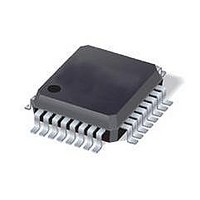
ST7FLI49MK1T6 STMicroelectronics, ST7FLI49MK1T6 Datasheet - Page 68

ST7FLI49MK1T6
Manufacturer Part Number
ST7FLI49MK1T6
Description
MCU 8BIT SGL VOLT FLASH 32-LQFP
Manufacturer
STMicroelectronics
Series
ST7r
Datasheet
1.ST7FLI49MK1T6TR.pdf
(187 pages)
Specifications of ST7FLI49MK1T6
Core Processor
ST7
Core Size
8-Bit
Speed
8MHz
Connectivity
I²C
Peripherals
LVD, POR, PWM, WDT
Number Of I /o
24
Program Memory Size
4KB (4K x 8)
Program Memory Type
FLASH
Eeprom Size
128 x 8
Ram Size
384 x 8
Voltage - Supply (vcc/vdd)
2.4 V ~ 5.5 V
Data Converters
A/D 10x10b
Oscillator Type
Internal
Operating Temperature
-40°C ~ 85°C
Package / Case
32-LQFP
Processor Series
ST7FLI4x
Core
ST7
Data Bus Width
8 bit
Data Ram Size
384 B
Interface Type
I2C
Maximum Clock Frequency
8 MHz
Number Of Programmable I/os
24
Number Of Timers
5
Maximum Operating Temperature
+ 125 C
Mounting Style
SMD/SMT
Minimum Operating Temperature
- 40 C
On-chip Adc
10 bit, 10 Channel
Lead Free Status / RoHS Status
Lead free / RoHS Compliant
Available stocks
Company
Part Number
Manufacturer
Quantity
Price
Company:
Part Number:
ST7FLI49MK1T6
Manufacturer:
st
Quantity:
456
Company:
Part Number:
ST7FLI49MK1T6
Manufacturer:
STMicroelectronics
Quantity:
10 000
Part Number:
ST7FLI49MK1T6
Manufacturer:
ST
Quantity:
20 000
Company:
Part Number:
ST7FLI49MK1T6TR
Manufacturer:
STMicroelectronics
Quantity:
10 000
I/O ports
10
10.1
10.2
10.2.1
Note:
68/188
1
2
I/O ports
Introduction
The I/O ports allow data transfer. An I/O port can contain up to 8 pins. Each pin can be
programmed independently either as a digital input or digital output. In addition, specific pins
may have several other functions. These functions can include external interrupt, alternate
signal input/output for on-chip peripherals or analog input.
Functional description
A data register (DR) and a data direction register (DDR) are always associated with each
port. The Option register (OR), which allows input/output options, may or may not be
implemented. The following description takes into account the OR register. Refer to the port
configuration table for device specific information.
An I/O pin is programmed using the corresponding bits in the DDR, DR and OR registers: bit
x corresponding to pin x of the port.
Figure 34
Input modes
Clearing the DDRx bit selects input mode. In this mode, reading its DR bit returns the digital
value from that I/O pin.
If an OR bit is available, different input modes can be configured by software: floating or pull-
up. Refer to I/O Port Implementation section for configuration.
Writing to the DR modifies the latch value but does not change the state of the input pin.
Do not use read/modify/write instructions (BSET/BRES) to modify the DR register.
External interrupt function
Depending on the device, setting the ORx bit while in input mode can configure an I/O as an
input with interrupt. In this configuration, a signal edge or level input on the I/O generates an
interrupt request via the corresponding interrupt vector (eix).
Falling or rising edge sensitivity is programmed independently for each interrupt vector. The
External Interrupt Control register (EICR) or the Miscellaneous register controls this
sensitivity, depending on the device.
Each external interrupt vector is linked to a dedicated group of I/O port pins (see pinout
description and interrupt section). If several I/O interrupt pins on the same interrupt vector
are selected simultaneously, they are logically combined. For this reason if one of the
interrupt pins is tied low, it may mask the others.
External interrupts are hardware interrupts. Fetching the corresponding interrupt vector
automatically clears the request latch. Changing the sensitivity of a particular external
interrupt clears this pending interrupt. This can be used to clear unwanted pending
interrupts.
shows the generic I/O block diagram.
Doc ID 13562 Rev 3
ST7LITE49M


