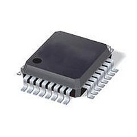
ST7FLI49MK1T6 STMicroelectronics, ST7FLI49MK1T6 Datasheet - Page 142

ST7FLI49MK1T6
Manufacturer Part Number
ST7FLI49MK1T6
Description
MCU 8BIT SGL VOLT FLASH 32-LQFP
Manufacturer
STMicroelectronics
Series
ST7r
Datasheet
1.ST7FLI49MK1T6TR.pdf
(187 pages)
Specifications of ST7FLI49MK1T6
Core Processor
ST7
Core Size
8-Bit
Speed
8MHz
Connectivity
I²C
Peripherals
LVD, POR, PWM, WDT
Number Of I /o
24
Program Memory Size
4KB (4K x 8)
Program Memory Type
FLASH
Eeprom Size
128 x 8
Ram Size
384 x 8
Voltage - Supply (vcc/vdd)
2.4 V ~ 5.5 V
Data Converters
A/D 10x10b
Oscillator Type
Internal
Operating Temperature
-40°C ~ 85°C
Package / Case
32-LQFP
Processor Series
ST7FLI4x
Core
ST7
Data Bus Width
8 bit
Data Ram Size
384 B
Interface Type
I2C
Maximum Clock Frequency
8 MHz
Number Of Programmable I/os
24
Number Of Timers
5
Maximum Operating Temperature
+ 125 C
Mounting Style
SMD/SMT
Minimum Operating Temperature
- 40 C
On-chip Adc
10 bit, 10 Channel
Lead Free Status / RoHS Status
Lead free / RoHS Compliant
Available stocks
Company
Part Number
Manufacturer
Quantity
Price
Company:
Part Number:
ST7FLI49MK1T6
Manufacturer:
st
Quantity:
456
Company:
Part Number:
ST7FLI49MK1T6
Manufacturer:
STMicroelectronics
Quantity:
10 000
Part Number:
ST7FLI49MK1T6
Manufacturer:
ST
Quantity:
20 000
Company:
Part Number:
ST7FLI49MK1T6TR
Manufacturer:
STMicroelectronics
Quantity:
10 000
Electrical characteristics
13.3
13.3.1
13.3.2
142/188
Operating conditions
General operating conditions
T
Table 61.
Figure 62. f
Operating conditions with low voltage detector (LVD)
T
Table 62.
1. Not tested in production. The V
A
A
,
NOT GUARANTEED
Symbol
Symbol
V
I
V
DD(LVD)
V
= -40 to 125 °C unless otherwise specified.
IT+
= -40 to +125 °C unless otherwise specified.
f
IT-
and LVD reset release. When the V
reset of the MCU.
V
V
FUNCTIONALITY
CPU
tPOR
hys
DD
(LVD)
(LVD)
IN THIS AREA
LVD voltage threshold hysteresis
General operating conditions
Operating characteristics with LVD
LVD/AVD current consumption
CPU
f
CPU clock frequency
Reset generation threshold
CPU
Reset release threshold
V
Supply voltage
8
4
2
0
[MHz]
maximum operating frequency versus V
DD
2.0
Parameter
rise time rate
Parameter
(V
(V
DD
2.4
DD
rise)
fall)
DD
2.7
Doc ID 13562 Rev 3
rise time rate condition is needed to ensure a correct device power-on
DD
3.3
(1)(2)
slope is outside these values, the LVD may not release properly the
3.5
f
f
2.4 V≤ V
3.3 V≤ V
CPU
CPU
V
Med. threshold
Med. threshold
High threshold
High threshold
Low threshold
Low threshold
IT+
Conditions
Conditions
4.0
V
= 4 MHz max.
= 8 MHz max.
(LVD)
DD
DD
DD
= 5 V
-V
< 3.3 V
≤ 5.5 V
IT-
4.5
(LVD)
DD
supply voltage
Min
5.0
3.9
3.2
2.5
3.7
3.0
2.4
2
Min
2.4
3.3
5.5
Typ
150
4.2
3.5
2.7
4.0
3.3
2.6
80
up to 8
up to 4
GUARANTEED
IN THIS AREA
(UNLESS OTHERWISE
STATED IN THE
TABLES OF
PARAMETRIC DATA)
FUNCTIONALITY
SUPPLY VOLTAGE [V]
ST7LITE49M
Max
Max
5.5
5.5
140
4.5
3.8
3.0
4.3
3.6
2.9
MHz
Unit
Unit
μs/V
mV
μA
V
V


