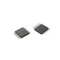
P89LPC9151FDH,129 NXP Semiconductors, P89LPC9151FDH,129 Datasheet - Page 60

P89LPC9151FDH,129
Manufacturer Part Number
P89LPC9151FDH,129
Description
IC 80C51 MCU FLASH 2KB 14TSSOP
Manufacturer
NXP Semiconductors
Series
LPC900r
Datasheet
1.P89LPC9151FDH129.pdf
(91 pages)
Specifications of P89LPC9151FDH,129
Program Memory Type
FLASH
Program Memory Size
2KB (2K x 8)
Package / Case
14-TSSOP
Core Processor
8051
Core Size
8-Bit
Speed
18MHz
Connectivity
I²C, UART/USART
Peripherals
Brown-out Detect/Reset, POR, PWM, WDT
Number Of I /o
12
Ram Size
256 x 8
Voltage - Supply (vcc/vdd)
2.4 V ~ 3.6 V
Data Converters
A/D 4x8b; D/A 1x8b
Oscillator Type
Internal
Operating Temperature
-40°C ~ 85°C
Processor Series
P89LPC
Core
80C51
Data Bus Width
8 bit
Data Ram Size
256 B
Interface Type
SPI
Maximum Clock Frequency
18 MHz
Number Of Programmable I/os
10
Number Of Timers
2
Operating Supply Voltage
2.4 V to 3.6 V
Maximum Operating Temperature
+ 85 C
Mounting Style
SMD/SMT
3rd Party Development Tools
PK51, CA51, A51, ULINK2
Minimum Operating Temperature
- 40 C
On-chip Adc
8 bit, 4 Channel
Lead Free Status / RoHS Status
Lead free / RoHS Compliant
Eeprom Size
-
Lead Free Status / Rohs Status
Lead free / RoHS Compliant
Other names
935290259129
NXP Semiconductors
8. ADC
P89LPC9151_61_71_2
Product data sheet
7.28.7 IAP-Lite
7.29 User configuration bytes
7.30 User sector security bytes
8.1 General description
8.2 Features
board area. The ICP function uses five pins. Only a small connector needs to be available
to interface your application to a commercial programmer in order to use this feature.
Additional details may be found in the P89LPC9151/9161/9171 User manual.
IAP-Lite is performed in the application under the control of the microcontroller’s firmware.
The IAP facility consists of internal hardware resources to facilitate programming and
erasing. The IAP-Lite operations are accomplished through the use of four SFRs
consisting of a control/status register, a data register, and two address registers.
Additional details may be found in the P89LPC9151/9161/9171 User’s Manual.
Some user-configurable features of the P89LPC9151/9161/9171 must be defined at
power-up and therefore cannot be set by the program after start of execution. These
features are configured through the use of the flash byte UCFG1 and UCFG2. Please see
the P89LPC9151/9161/9171 User’s Manual for additional details.
There are 8 User Sector Security Bytes on the P89LPC9151/9161/9171. Each byte
corresponds to one sector. Please see the P89LPC9151/9161/9171 User manual for
additional details.
The P89LPC9151/9161/9171 devices have a single 8-bit, 4-channel multiplexed
analog-to-digital converter. A block diagram of the A/D converter is shown in
The A/D consists of a 4-input multiplexer which feeds a sample-and-hold circuit providing
an input signal to one of two comparator inputs. The control logic in combination with the
SAR drives a digital-to-analog converter which provides the other input to the comparator.
The output of the comparator is fed to the SAR.
8-bit, 4-channel multiplexed input, successive approximation ADC.
Four A/D result registers.
Six operating modes:
Three conversion start modes:
Fixed channel, single conversion mode.
Fixed channel, continuous conversion mode.
Auto scan, single conversion mode.
Auto scan, continuous conversion mode.
Dual channel, continuous conversion mode.
Single step mode.
Timer triggered start.
Start immediately.
Rev. 02 — 9 February 2010
P89LPC9151/9161/9171
8-bit microcontroller with 8-bit ADC
© NXP B.V. 2010. All rights reserved.
Figure
60 of 91
21.


