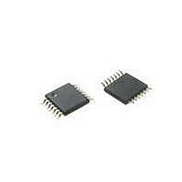
P89LPC9151FDH,129 NXP Semiconductors, P89LPC9151FDH,129 Datasheet - Page 44

P89LPC9151FDH,129
Manufacturer Part Number
P89LPC9151FDH,129
Description
IC 80C51 MCU FLASH 2KB 14TSSOP
Manufacturer
NXP Semiconductors
Series
LPC900r
Datasheet
1.P89LPC9151FDH129.pdf
(91 pages)
Specifications of P89LPC9151FDH,129
Program Memory Type
FLASH
Program Memory Size
2KB (2K x 8)
Package / Case
14-TSSOP
Core Processor
8051
Core Size
8-Bit
Speed
18MHz
Connectivity
I²C, UART/USART
Peripherals
Brown-out Detect/Reset, POR, PWM, WDT
Number Of I /o
12
Ram Size
256 x 8
Voltage - Supply (vcc/vdd)
2.4 V ~ 3.6 V
Data Converters
A/D 4x8b; D/A 1x8b
Oscillator Type
Internal
Operating Temperature
-40°C ~ 85°C
Processor Series
P89LPC
Core
80C51
Data Bus Width
8 bit
Data Ram Size
256 B
Interface Type
SPI
Maximum Clock Frequency
18 MHz
Number Of Programmable I/os
10
Number Of Timers
2
Operating Supply Voltage
2.4 V to 3.6 V
Maximum Operating Temperature
+ 85 C
Mounting Style
SMD/SMT
3rd Party Development Tools
PK51, CA51, A51, ULINK2
Minimum Operating Temperature
- 40 C
On-chip Adc
8 bit, 4 Channel
Lead Free Status / RoHS Status
Lead free / RoHS Compliant
Eeprom Size
-
Lead Free Status / Rohs Status
Lead free / RoHS Compliant
Other names
935290259129
NXP Semiconductors
P89LPC9151_61_71_2
Product data sheet
7.15.1.1 Quasi-bidirectional output configuration
7.15.1 Port configurations
7.15 I/O ports
The P89LPC9151 has two I/O ports: Port 0 and Port 1. Ports 0 and 1 are both 6-bit ports.
The P89LPC9161/9171 has three I/O ports: Port 0, Port 1 and Port 2. Ports 0 is 5-bit ports
in the P89LPC9161 and 7-bit ports in the P89LPC9171, Port 1 is 5-bit ports in the
P89LPC9161 and 6-bit ports in the P89LPC9171, Port 2 is 4-bit ports in the P89LPC9161
and 1-bit port in the P89LPC9171. The exact number of I/O pins available depends upon
the clock and reset options chosen, as shown in
Table 13.
[1]
Table 14.
[1]
All but three I/O port pins on the P89LPC9151/9161/9171 may be configured by software
to one of four types on a bit-by-bit basis. These are: quasi-bidirectional (standard 80C51
port outputs), push-pull, open drain, and input-only. Two configuration registers for each
port select the output type for each port pin.
Quasi-bidirectional output type can be used as both an input and output without the need
to reconfigure the port. This is possible because when the port outputs a logic HIGH, it is
weakly driven, allowing an external device to pull the pin LOW. When the pin is driven
Clock source
RC oscillator or watchdog
oscillator
External clock input
Clock source
RC oscillator or watchdog
oscillator
External clock input
1. P1.5 (RST) can only be an input and cannot be configured.
2. P1.2 (SCL/T0) and P1.3 (SDA/INT0) may only be configured to be either input-only or
Required for operation above 12 MHz.
Required for operation above 12 MHz.
open-drain.
Number of I/O pins available (P89LPC9151)
Number of I/O pins available (P89LPC9161 and P89LPC9171)
Rev. 02 — 9 February 2010
Reset option
No external reset (except during
power-up)
External RST pin supported
No external reset (except during
power-up)
External RST pin supported
Reset option
No external reset (except during
power-up)
External RST pin supported
No external reset (except during
power-up)
External RST pin supported
P89LPC9151/9161/9171
Table 13
8-bit microcontroller with 8-bit ADC
[1]
[1]
and
Table 14
© NXP B.V. 2010. All rights reserved.
Number of I/O
pins (14-pin
package)
12
11
11
10
Number of I/O
pins (16-pin
package)
14
13
13
12
44 of 91


