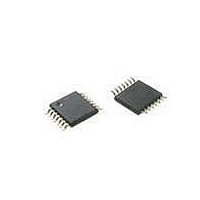
P89LPC9151FDH,129 NXP Semiconductors, P89LPC9151FDH,129 Datasheet - Page 38

P89LPC9151FDH,129
Manufacturer Part Number
P89LPC9151FDH,129
Description
IC 80C51 MCU FLASH 2KB 14TSSOP
Manufacturer
NXP Semiconductors
Series
LPC900r
Datasheet
1.P89LPC9151FDH129.pdf
(91 pages)
Specifications of P89LPC9151FDH,129
Program Memory Type
FLASH
Program Memory Size
2KB (2K x 8)
Package / Case
14-TSSOP
Core Processor
8051
Core Size
8-Bit
Speed
18MHz
Connectivity
I²C, UART/USART
Peripherals
Brown-out Detect/Reset, POR, PWM, WDT
Number Of I /o
12
Ram Size
256 x 8
Voltage - Supply (vcc/vdd)
2.4 V ~ 3.6 V
Data Converters
A/D 4x8b; D/A 1x8b
Oscillator Type
Internal
Operating Temperature
-40°C ~ 85°C
Processor Series
P89LPC
Core
80C51
Data Bus Width
8 bit
Data Ram Size
256 B
Interface Type
SPI
Maximum Clock Frequency
18 MHz
Number Of Programmable I/os
10
Number Of Timers
2
Operating Supply Voltage
2.4 V to 3.6 V
Maximum Operating Temperature
+ 85 C
Mounting Style
SMD/SMT
3rd Party Development Tools
PK51, CA51, A51, ULINK2
Minimum Operating Temperature
- 40 C
On-chip Adc
8 bit, 4 Channel
Lead Free Status / RoHS Status
Lead free / RoHS Compliant
Eeprom Size
-
Lead Free Status / Rohs Status
Lead free / RoHS Compliant
Other names
935290259129
NXP Semiconductors
P89LPC9151_61_71_2
Product data sheet
7.3.1 Clock definitions
7.3.2 CPU clock (OSCCLK)
7.2 Enhanced CPU
7.3 Clocks
7.4 Clock output (P89LPC9171)
7.5 On-chip RC oscillator option
The P89LPC9151/9161/9171 uses an enhanced 80C51 CPU which runs at six times the
speed of standard 80C51 devices. A machine cycle consists of two CPU clock cycles, and
most instructions execute in one or two machine cycles.
The P89LPC9151/9161/9171 device has several internal clocks as defined below:
OSCCLK — Input to the DIVM clock divider. OSCCLK is selected from one of four clock
sources (see
Section 7.10 “CCLK modification: DIVM
Remark: f
CCLK — CPU clock; output of the clock divider. There are two CCLK cycles per machine
cycle, and most instructions are executed in one to two machine cycles (two or four CCLK
cycles).
RCCLK — The internal 7.373 MHz RC oscillator output. The clock doubler option, when
enabled, provides an output frequency of 14.746 MHz.
PCLK — Clock for the various peripheral devices and is
The P89LPC9151/9161/9171 provides several user-selectable oscillator options in
generating the CPU clock. This allows optimization for a range of needs from high
precision to lowest possible cost. These options are configured when the flash is
programmed and include an on-chip watchdog oscillator, an on-chip RC oscillator, or an
external clock source.
The P89LPC9171 supports a user-selectable clock output function on the P0.7/CLKOUT
pin. This allows external devices to synchronize to the P89LPC9171. This output is
enabled by the ENCLK bit in the TRIM register.
The frequency of this clock output is
in Idle mode, it may be turned off prior to entering Idle, saving additional power.
The P89LPC9151/9161/9171 has a 6-bit TRIM register that can be used to tune the
frequency of the RC oscillator. During reset, the TRIM value is initialized to a factory
preprogrammed value to adjust the oscillator frequency to 7.373 MHz ± 1 % at room
temperature. End-user applications can write to the TRIM register to adjust the on-chip
RC oscillator to other frequencies. When the clock doubler option is enabled (UCFG2.7 =
1), the output frequency is 14.746 MHz. If CCLK is 8 MHz or slower, the CLKLP SFR bit
(AUXR1.7) can be set to logic 1 to reduce power consumption. On reset, CLKLP is logic 0
allowing highest performance access. This bit can then be set in software if CCLK is
osc
Figure
is defined as the OSCCLK frequency.
10) and can also be optionally divided to a slower frequency (see
Rev. 02 — 9 February 2010
1
⁄
2
that of the CCLK. If the clock output is not needed
P89LPC9151/9161/9171
register”).
8-bit microcontroller with 8-bit ADC
CCLK
⁄
2
.
© NXP B.V. 2010. All rights reserved.
38 of 91


