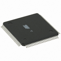
ATMEGA2560V-8AU Atmel, ATMEGA2560V-8AU Datasheet - Page 126

ATMEGA2560V-8AU
Manufacturer Part Number
ATMEGA2560V-8AU
Description
IC AVR MCU 256K 8MHZ 100TQFP
Manufacturer
Atmel
Series
AVR® ATmegar
Datasheets
1.ATMEGA640V-8CU.pdf
(38 pages)
2.ATMEGA640V-8CU.pdf
(444 pages)
3.ATMEGA2560V-8AU.pdf
(37 pages)
Specifications of ATMEGA2560V-8AU
Core Processor
AVR
Core Size
8-Bit
Speed
8MHz
Connectivity
EBI/EMI, I²C, SPI, UART/USART
Peripherals
Brown-out Detect/Reset, POR, PWM, WDT
Number Of I /o
86
Program Memory Size
256KB (128K x 16)
Program Memory Type
FLASH
Eeprom Size
4K x 8
Ram Size
8K x 8
Voltage - Supply (vcc/vdd)
1.8 V ~ 5.5 V
Data Converters
A/D 16x10b
Oscillator Type
Internal
Operating Temperature
-40°C ~ 85°C
Package / Case
100-TQFP, 100-VQFP
Processor Series
ATMEGA256x
Core
AVR8
Data Bus Width
8 bit
Data Ram Size
8 KB
Interface Type
2-Wire, SPI, USART
Maximum Clock Frequency
8 MHz
Number Of Programmable I/os
86
Number Of Timers
6
Operating Supply Voltage
1.8 V to 5.5 V
Maximum Operating Temperature
+ 85 C
Mounting Style
SMD/SMT
3rd Party Development Tools
EWAVR, EWAVR-BL
Minimum Operating Temperature
- 40 C
On-chip Adc
10 bit, 16 Channel
A/d Inputs
16-Channel, 10-Bit
Cpu Speed
8 MIPS
Eeprom Memory
4K Bytes
Input Output
86
Interface
2-Wire/SPI/USART
Memory Type
Flash
Number Of Bits
8
Package Type
100-pin TQFP
Programmable Memory
256K Bytes
Timers
2-8-bit, 4-16-bit
Voltage, Range
1.8-5.5 V
Package
100TQFP
Device Core
AVR
Family Name
ATmega
Maximum Speed
8 MHz
For Use With
ATSTK600-TQFP100 - STK600 SOCKET/ADAPTER 100-TQFP770-1007 - ISP 4PORT ATMEL AVR MCU SPI/JTAG770-1005 - ISP 4PORT FOR ATMEL AVR MCU JTAG770-1004 - ISP 4PORT FOR ATMEL AVR MCU SPIATAVRISP2 - PROGRAMMER AVR IN SYSTEMATSTK503 - STARTER KIT AVR EXP MODULE 100PATJTAGICE2 - AVR ON-CHIP D-BUG SYSTEM
Lead Free Status / RoHS Status
Lead free / RoHS Compliant
Available stocks
Company
Part Number
Manufacturer
Quantity
Price
Company:
Part Number:
ATMEGA2560V-8AU
Manufacturer:
Atmel
Quantity:
900
Part Number:
ATMEGA2560V-8AU
Manufacturer:
ATMEL/爱特梅尔
Quantity:
20 000
- Current page: 126 of 444
- Download datasheet (10Mb)
15.7.4
2549M–AVR–09/10
Phase Correct PWM Mode
The phase correct PWM mode (WGM02:0 = 1 or 5) provides a high resolution phase correct
PWM waveform generation option. The phase correct PWM mode is based on a dual-slope
operation. The counter counts repeatedly from BOTTOM to TOP and then from TOP to BOT-
TOM. TOP is defined as 0xFF when WGM2:0 = 1, and OCR0A when WGM2:0 = 5. In non-
inverting Compare Output mode, the Output Compare (OC0x) is cleared on the Compare Match
between TCNT0 and OCR0x while upcounting, and set on the Compare Match while down-
counting. In inverting Output Compare mode, the operation is inverted. The dual-slope operation
has lower maximum operation frequency than single slope operation. However, due to the sym-
metric feature of the dual-slope PWM modes, these modes are preferred for motor control
applications.
In phase correct PWM mode the counter is incremented until the counter value matches TOP.
When the counter reaches TOP, it changes the count direction. The TCNT0 value will be equal
to TOP for one timer clock cycle. The timing diagram for the phase correct PWM mode is shown
on
the dual-slope operation. The diagram includes non-inverted and inverted PWM outputs. The
small horizontal line marks on the TCNT0 slopes represent Compare Matches between OCR0x
and TCNT0.
Figure 15-7. Phase Correct PWM Mode, Timing Diagram
The Timer/Counter Overflow Flag (TOV0) is set each time the counter reaches BOTTOM. The
Interrupt Flag can be used to generate an interrupt each time the counter reaches the BOTTOM
value.
In phase correct PWM mode, the compare unit allows generation of PWM waveforms on the
OC0x pins. Setting the COM0x1:0 bits to two will produce a non-inverted PWM. An inverted
PWM output can be generated by setting the COM0x1:0 to three: Setting the COM0A0 bits to
one allows the OC0A pin to toggle on Compare Matches if the WGM02 bit is set. This option is
not available for the OC0B pin (see
visible on the port pin if the data direction for the port pin is set as output. The PWM waveform is
Figure
TCNTn
OCnx
OCnx
Period
15-7. The TCNT0 value is in the timing diagram shown as a histogram for illustrating
1
ATmega640/1280/1281/2560/2561
Table 15-4 on page
2
130). The actual OC0x value will only be
3
OCnx Interrupt Flag Set
OCRnx Update
TOVn Interrupt Flag Set
(COMnx1:0 = 2)
(COMnx1:0 = 3)
126
Related parts for ATMEGA2560V-8AU
Image
Part Number
Description
Manufacturer
Datasheet
Request
R

Part Number:
Description:
IC AVR MCU 2.4GHZ XCEIVER 64QFN
Manufacturer:
Atmel
Datasheet:

Part Number:
Description:
Manufacturer:
Atmel
Datasheet:

Part Number:
Description:
MCU ATMEGA644/AT86RF230 40-DIP
Manufacturer:
Atmel
Datasheet:

Part Number:
Description:
BUNDLE ATMEGA644P/AT86RF230 QFN
Manufacturer:
Atmel
Datasheet:

Part Number:
Description:
BUNDLE ATMEGA644P/AT86RF230 TQFP
Manufacturer:
Atmel
Datasheet:

Part Number:
Description:
MCU ATMEGA1281/AT86RF230 64-TQFP
Manufacturer:
Atmel
Datasheet:

Part Number:
Description:
MCU ATMEGA1280/AT86RF230 100TQFP
Manufacturer:
Atmel
Datasheet:

Part Number:
Description:
BUNDLE ATMEGA1280/AT86RF100-TQFP
Manufacturer:
Atmel
Datasheet:

Part Number:
Description:
BUNDLE ATMEGA2560V/AT86RF230-ZU
Manufacturer:
Atmel
Datasheet:

Part Number:
Description:
MCU ATMEGA2561/AT86RF230 64-TQFP
Manufacturer:
Atmel
Datasheet:

Part Number:
Description:
INTERVAL AND WIPE/WASH WIPER CONTROL IC WITH DELAY
Manufacturer:
ATMEL Corporation
Datasheet:

Part Number:
Description:
Low-Voltage Voice-Switched IC for Hands-Free Operation
Manufacturer:
ATMEL Corporation
Datasheet:

Part Number:
Description:
MONOLITHIC INTEGRATED FEATUREPHONE CIRCUIT
Manufacturer:
ATMEL Corporation
Datasheet:

Part Number:
Description:
AM-FM Receiver IC U4255BM-M
Manufacturer:
ATMEL Corporation
Datasheet:


