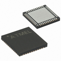
ATMEGA162-16MU Atmel, ATMEGA162-16MU Datasheet - Page 78

ATMEGA162-16MU
Manufacturer Part Number
ATMEGA162-16MU
Description
IC AVR MCU 16K 16MHZ 5V 44-QFN
Manufacturer
Atmel
Series
AVR® ATmegar
Specifications of ATMEGA162-16MU
Core Processor
AVR
Core Size
8-Bit
Speed
16MHz
Connectivity
EBI/EMI, SPI, UART/USART
Peripherals
Brown-out Detect/Reset, POR, PWM, WDT
Number Of I /o
35
Program Memory Size
16KB (8K x 16)
Program Memory Type
FLASH
Eeprom Size
512 x 8
Ram Size
1K x 8
Voltage - Supply (vcc/vdd)
2.7 V ~ 5.5 V
Oscillator Type
Internal
Operating Temperature
-40°C ~ 85°C
Package / Case
44-VQFN Exposed Pad
Processor Series
ATMEGA16x
Core
AVR8
Data Bus Width
8 bit
Data Ram Size
1 KB
Interface Type
JTAG/SPI/USART
Maximum Clock Frequency
16 MHz
Number Of Programmable I/os
35
Number Of Timers
4
Operating Supply Voltage
2.7 V to 5.5 V
Maximum Operating Temperature
+ 85 C
Mounting Style
SMD/SMT
3rd Party Development Tools
EWAVR, EWAVR-BL
Development Tools By Supplier
ATAVRDRAGON, ATSTK500, ATSTK600, ATAVRISP2, ATAVRONEKIT
Minimum Operating Temperature
- 40 C
Package
44MLF EP
Device Core
AVR
Family Name
ATmega
Maximum Speed
16 MHz
Controller Family/series
AVR MEGA
No. Of I/o's
35
Eeprom Memory Size
512Byte
Ram Memory Size
1KB
Cpu Speed
16MHz
Rohs Compliant
Yes
For Use With
ATSTK600-TQFP44 - STK600 SOCKET/ADAPTER 44-TQFPATSTK600 - DEV KIT FOR AVR/AVR32770-1007 - ISP 4PORT ATMEL AVR MCU SPI/JTAGATAVRISP2 - PROGRAMMER AVR IN SYSTEMATJTAGICE2 - AVR ON-CHIP D-BUG SYSTEMATSTK500 - PROGRAMMER AVR STARTER KIT
Lead Free Status / RoHS Status
Lead free / RoHS Compliant
Data Converters
-
Lead Free Status / Rohs Status
Lead free / RoHS Compliant
Available stocks
Company
Part Number
Manufacturer
Quantity
Price
Part Number:
ATMEGA162-16MU
Manufacturer:
QFN
Quantity:
20 000
- Current page: 78 of 324
- Download datasheet (6Mb)
Alternate Functions of
Port D
78
ATmega162/V
The Port D pins with alternate functions are shown in
Table 38. Port D Pins Alternate Functions
The alternate pin configuration is as follows:
• RD – Port D, Bit 7
RD is the external data memory read control strobe.
• WR – Port D, Bit 6
WR is the external data memory write control strobe.
• TOSC2/OC1A – Port D, Bit 5
TOSC2, Timer Oscillator pin 2: When the AS2 bit in ASSR is set (one) to enable asynchronous
clocking of Timer/Counter2, pin PD5 is disconnected from the port, and becomes the inverting
output of the Oscillator amplifier. In this mode, a crystal Oscillator is connected to this pin, and
the pin can not be used as an I/O pin.
OC1A, Output Compare Match A output: The PD5 pin can serve as an external output for the
Timer/Counter1 Output Compare A. The pin has to be configured as an output (DDD5 set (one))
to serve this function. The OC1A pin is also the output pin for the PWM mode timer function.
Port Pin
PD7
PD6
PD5
PD4
PD3
PD2
PD1
PD0
Alternate Function
RD (Read strobe to external memory)
WR (Write strobe to external memory)
TOSC2 (Timer Oscillator Pin 2)
OC1A (Timer/Counter1 Output Compare A Match Output)
TOSC1 (Timer Oscillator Pin 1)
XCK0 (USART0 External Clock Input/Output)
OC3A (Timer/Counter3 Output Compare A Match Output)
INT1 (External Interrupt 1 Input)
ICP3 (Timer/Counter3 Input Capture Pin)
INT0 (External Interrupt 0 Input)
XCK1 (USART1 External Clock Input/Output)
TXD0 (USART0 Output Pin)
RXD0 (USART0 Input Pin)
Table
38.
2513K–AVR–07/09
Related parts for ATMEGA162-16MU
Image
Part Number
Description
Manufacturer
Datasheet
Request
R

Part Number:
Description:
Manufacturer:
Atmel Corporation
Datasheet:

Part Number:
Description:
IC AVR MCU 16K 16MHZ 5V 44TQFP
Manufacturer:
Atmel
Datasheet:

Part Number:
Description:
IC AVR MCU 16K 16MHZ 5V 40DIP
Manufacturer:
Atmel
Datasheet:

Part Number:
Description:
IC MCU AVR 16K 5V 16MHZ 44-TQFP
Manufacturer:
Atmel
Datasheet:

Part Number:
Description:
IC MCU AVR 16K 5V 16MHZ 44-QFN
Manufacturer:
Atmel
Datasheet:

Part Number:
Description:
MCU AVR 16KB FLASH 16MHZ 44QFN
Manufacturer:
Atmel
Datasheet:

Part Number:
Description:
MCU AVR 16KB FLASH 16MHZ 44TQFP
Manufacturer:
Atmel
Datasheet:

Part Number:
Description:
IC MCU AVR 16K 5V 16MHZ 44-TQFP
Manufacturer:
Atmel
Datasheet:

Part Number:
Description:
IC MCU AVR 16K 5V 16MHZ 44-QFN
Manufacturer:
Atmel
Datasheet:

Part Number:
Description:
IC MCU AVR 16K 5V 16MHZ 40-DIP
Manufacturer:
Atmel
Datasheet:

Part Number:
Description:
IC MCU AVR 16K 5V 16MHZ 40-DIP
Manufacturer:
Atmel
Datasheet:

Part Number:
Description:
IC MCU AVR 16K 5V 16MHZ 44-TQFP
Manufacturer:
Atmel
Datasheet:

Part Number:
Description:
IC MCU AVR 16K 5V 16MHZ 44-QFN
Manufacturer:
Atmel
Datasheet:


