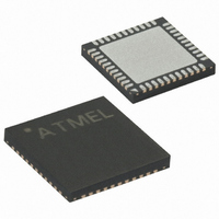
ATMEGA162-16MU Atmel, ATMEGA162-16MU Datasheet - Page 147

ATMEGA162-16MU
Manufacturer Part Number
ATMEGA162-16MU
Description
IC AVR MCU 16K 16MHZ 5V 44-QFN
Manufacturer
Atmel
Series
AVR® ATmegar
Specifications of ATMEGA162-16MU
Core Processor
AVR
Core Size
8-Bit
Speed
16MHz
Connectivity
EBI/EMI, SPI, UART/USART
Peripherals
Brown-out Detect/Reset, POR, PWM, WDT
Number Of I /o
35
Program Memory Size
16KB (8K x 16)
Program Memory Type
FLASH
Eeprom Size
512 x 8
Ram Size
1K x 8
Voltage - Supply (vcc/vdd)
2.7 V ~ 5.5 V
Oscillator Type
Internal
Operating Temperature
-40°C ~ 85°C
Package / Case
44-VQFN Exposed Pad
Processor Series
ATMEGA16x
Core
AVR8
Data Bus Width
8 bit
Data Ram Size
1 KB
Interface Type
JTAG/SPI/USART
Maximum Clock Frequency
16 MHz
Number Of Programmable I/os
35
Number Of Timers
4
Operating Supply Voltage
2.7 V to 5.5 V
Maximum Operating Temperature
+ 85 C
Mounting Style
SMD/SMT
3rd Party Development Tools
EWAVR, EWAVR-BL
Development Tools By Supplier
ATAVRDRAGON, ATSTK500, ATSTK600, ATAVRISP2, ATAVRONEKIT
Minimum Operating Temperature
- 40 C
Package
44MLF EP
Device Core
AVR
Family Name
ATmega
Maximum Speed
16 MHz
Controller Family/series
AVR MEGA
No. Of I/o's
35
Eeprom Memory Size
512Byte
Ram Memory Size
1KB
Cpu Speed
16MHz
Rohs Compliant
Yes
For Use With
ATSTK600-TQFP44 - STK600 SOCKET/ADAPTER 44-TQFPATSTK600 - DEV KIT FOR AVR/AVR32770-1007 - ISP 4PORT ATMEL AVR MCU SPI/JTAGATAVRISP2 - PROGRAMMER AVR IN SYSTEMATJTAGICE2 - AVR ON-CHIP D-BUG SYSTEMATSTK500 - PROGRAMMER AVR STARTER KIT
Lead Free Status / RoHS Status
Lead free / RoHS Compliant
Data Converters
-
Lead Free Status / Rohs Status
Lead free / RoHS Compliant
Available stocks
Company
Part Number
Manufacturer
Quantity
Price
Part Number:
ATMEGA162-16MU
Manufacturer:
QFN
Quantity:
20 000
- Current page: 147 of 324
- Download datasheet (6Mb)
Timer/Counter
Timing Diagrams
2513K–AVR–07/09
actual OC2 value will only be visible on the port pin if the data direction for the port pin is set as
output. The PWM waveform is generated by clearing (or setting) the OC2 Register at the Com-
pare Match between OCR2 and TCNT2 when the counter increments, and setting (or clearing)
the OC2 Register at Compare Match between OCR2 and TCNT2 when the counter decrements.
The PWM frequency for the output when using phase correct PWM can be calculated by the fol-
lowing equation:
The N variable represents the prescale factor (1, 8, 32, 64, 128, 256, or 1024).
The extreme values for the OCR2 Register represent special cases when generating a PWM
waveform output in the phase correct PWM mode. If the OCR2 is set equal to BOTTOM, the out-
put will be continuously low and if set equal to MAX the output will be continuously high for non-
inverted PWM mode. For inverted PWM the output will have the opposite logic values.
At the very start of period 2 in
is no Compare Match. The point of this transition is to guarantee symmetry around BOTTOM.
There are two cases that give a transition without a Compare Match.
•
•
The following figures show the Timer/Counter in synchronous mode, and the timer clock (clk
is therefore shown as a clock enable signal. In asynchronous mode, clk
the Timer/Counter Oscillator clock. The figures include information on when Interrupt Flags are
set.
count sequence close to the MAX value in all modes other than phase correct PWM mode.
Figure 66. Timer/Counter Timing Diagram, no Prescaling
Figure 67
OCR2 changes its value from MAX, like in
OCn pin value is the same as the result of a down-counting Compare Match. To ensure
symmetry around BOTTOM the OCn value at MAX must correspond to the result of an up-
counting Compare Match.
The timer starts counting from a value higher than the one in OCR2, and for that reason
misses the Compare Match and hence the OCn change that would have happened on the
way up.
Figure 66
TCNTn
(clk
TOVn
clk
clk
shows the same timing data, but with the prescaler enabled.
I/O
I/O
Tn
/1)
contains timing data for basic Timer/Counter operation. The figure shows the
MAX - 1
Figure 65
f
OCnPCPWM
OCn has a transition from high to low even though there
MAX
Figure
=
----------------- -
N 510
f
clk_I/O
⋅
65. When the OCR2 value is MAX the
BOTTOM
ATmega162/V
I/O
should be replaced by
BOTTOM + 1
147
T
2)
Related parts for ATMEGA162-16MU
Image
Part Number
Description
Manufacturer
Datasheet
Request
R

Part Number:
Description:
Manufacturer:
Atmel Corporation
Datasheet:

Part Number:
Description:
IC AVR MCU 16K 16MHZ 5V 44TQFP
Manufacturer:
Atmel
Datasheet:

Part Number:
Description:
IC AVR MCU 16K 16MHZ 5V 40DIP
Manufacturer:
Atmel
Datasheet:

Part Number:
Description:
IC MCU AVR 16K 5V 16MHZ 44-TQFP
Manufacturer:
Atmel
Datasheet:

Part Number:
Description:
IC MCU AVR 16K 5V 16MHZ 44-QFN
Manufacturer:
Atmel
Datasheet:

Part Number:
Description:
MCU AVR 16KB FLASH 16MHZ 44QFN
Manufacturer:
Atmel
Datasheet:

Part Number:
Description:
MCU AVR 16KB FLASH 16MHZ 44TQFP
Manufacturer:
Atmel
Datasheet:

Part Number:
Description:
IC MCU AVR 16K 5V 16MHZ 44-TQFP
Manufacturer:
Atmel
Datasheet:

Part Number:
Description:
IC MCU AVR 16K 5V 16MHZ 44-QFN
Manufacturer:
Atmel
Datasheet:

Part Number:
Description:
IC MCU AVR 16K 5V 16MHZ 40-DIP
Manufacturer:
Atmel
Datasheet:

Part Number:
Description:
IC MCU AVR 16K 5V 16MHZ 40-DIP
Manufacturer:
Atmel
Datasheet:

Part Number:
Description:
IC MCU AVR 16K 5V 16MHZ 44-TQFP
Manufacturer:
Atmel
Datasheet:

Part Number:
Description:
IC MCU AVR 16K 5V 16MHZ 44-QFN
Manufacturer:
Atmel
Datasheet:


