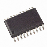
ATTINY861-20SU Atmel, ATTINY861-20SU Datasheet - Page 97

ATTINY861-20SU
Manufacturer Part Number
ATTINY861-20SU
Description
IC MCU AVR 8K FLASH 20MHZ 20SOIC
Manufacturer
Atmel
Series
AVR® ATtinyr
Datasheet
1.ATAVRMC321.pdf
(242 pages)
Specifications of ATTINY861-20SU
Core Processor
AVR
Core Size
8-Bit
Speed
20MHz
Connectivity
USI
Peripherals
Brown-out Detect/Reset, POR, PWM, WDT
Number Of I /o
16
Program Memory Size
8KB (4K x 16)
Program Memory Type
FLASH
Eeprom Size
512 x 8
Ram Size
512 x 8
Voltage - Supply (vcc/vdd)
2.7 V ~ 5.5 V
Data Converters
A/D 11x10b
Oscillator Type
Internal
Operating Temperature
-40°C ~ 85°C
Package / Case
20-SOIC (7.5mm Width)
Cpu Family
ATtiny
Device Core
AVR
Device Core Size
8b
Frequency (max)
20MHz
Interface Type
USI
Total Internal Ram Size
512Byte
# I/os (max)
16
Number Of Timers - General Purpose
2
Operating Supply Voltage (typ)
3.3/5V
Operating Supply Voltage (max)
5.5V
Operating Supply Voltage (min)
2.7V
On-chip Adc
11-chx10-bit
Instruction Set Architecture
RISC
Operating Temp Range
-40C to 85C
Operating Temperature Classification
Industrial
Mounting
Surface Mount
Pin Count
20
Package Type
SOIC
Processor Series
ATTINY8x
Core
AVR8
Data Bus Width
8 bit
Data Ram Size
512 B
Maximum Clock Frequency
20 MHz
Number Of Programmable I/os
16
Number Of Timers
2
Operating Supply Voltage
2.7 V to 5.5 V
Maximum Operating Temperature
+ 85 C
Mounting Style
SMD/SMT
3rd Party Development Tools
EWAVR, EWAVR-BL
Development Tools By Supplier
ATAVRDRAGON, ATSTK500, ATSTK600, ATAVRISP2, ATAVRONEKIT, ATAVRMC320
Minimum Operating Temperature
- 40 C
For Use With
ATSTK600 - DEV KIT FOR AVR/AVR32ATAVRBC100 - REF DESIGN KIT BATTERY CHARGER770-1007 - ISP 4PORT ATMEL AVR MCU SPI/JTAG770-1004 - ISP 4PORT FOR ATMEL AVR MCU SPI
Lead Free Status / RoHS Status
Lead free / RoHS Compliant
Available stocks
Company
Part Number
Manufacturer
Quantity
Price
12.7
2588E–AVR–08/10
Compare Match Output Unit
zero. The outputs OC1x and OC1x are inverted, if the PWM Inversion Mode bit PWM1X is set.
This will also cause both outputs to be high during the dead time.
The length of the counting period is user adjustable by selecting the dead time prescaler setting
by using the DTPS11:10 control bits, and selecting then the dead time value in I/O register DT1.
The DT1 register consists of two 4-bit fields, DT1H and DT1L that control the dead time periods
of the PWM output and its' complementary output separately in terms of the number of pres-
caled dead time generator clock cycles. Thus the rising edge of OC1x and OC1x can have
different dead time periods as the t
t
Figure 12-9. The Complementary Output Pair, COM1x1:0 = 1
The Compare Output Mode (COM1x1:0) bits have two functions. The Waveform Generator uses
the COM1x1:0 bits for defining the inverted or non-inverted Waveform Output (OCW1x) at the
next Compare Match. Also, the COM1x1:0 bits control the OC1x and OC1x pin output source.
Figure 12-10 on page 98
setting. The I/O Registers, I/O bits, and I/O pins in the figure are shown in bold. Only the parts of
the general I/O Port Control Registers (DDR and PORT) that are affected by the COM1x1:0 bits
are shown.
In Normal Mode (non-PWM) the Dead Time Generator is disabled and it is working like a syn-
chronizer: the Output Compare (OC1x) is delayed from the Waveform Output (OCW1x) by one
timer clock cycle. Whereas in Fast PWM Mode and in Phase and Frequency Correct PWM
Mode when the COM1x1:0 bits are set to “01” both the non-inverted and the inverted Output
Compare output are generated, and an user programmable Dead Time delay is inserted for
these complementary output pairs (OC1x and OC1x). The functionality in PWM modes is similar
to Normal mode when any other COM1x1:0 bit setup is used. When referring to the OC1x state,
the reference is for the Output Compare output (OC1x) from the Dead Time Generator, not the
OC1x pin. If a system reset occur, the OC1x is reset to “0”.
non-overlap / falling edge
OCWnx
OCnx
OCnx
(COMnx = 1)
t
non-overlap / rising edge
is adjusted by the 4-bit DT1L value.
shows a simplified schematic of the logic affected by the COM1x1:0 bit
t
non-overlap / falling edge
non-overlap / rising edge
is adjusted by the 4-bit DT1H value and the
97


