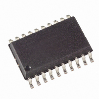
ATTINY861-20SU Atmel, ATTINY861-20SU Datasheet - Page 69

ATTINY861-20SU
Manufacturer Part Number
ATTINY861-20SU
Description
IC MCU AVR 8K FLASH 20MHZ 20SOIC
Manufacturer
Atmel
Series
AVR® ATtinyr
Datasheet
1.ATAVRMC321.pdf
(242 pages)
Specifications of ATTINY861-20SU
Core Processor
AVR
Core Size
8-Bit
Speed
20MHz
Connectivity
USI
Peripherals
Brown-out Detect/Reset, POR, PWM, WDT
Number Of I /o
16
Program Memory Size
8KB (4K x 16)
Program Memory Type
FLASH
Eeprom Size
512 x 8
Ram Size
512 x 8
Voltage - Supply (vcc/vdd)
2.7 V ~ 5.5 V
Data Converters
A/D 11x10b
Oscillator Type
Internal
Operating Temperature
-40°C ~ 85°C
Package / Case
20-SOIC (7.5mm Width)
Cpu Family
ATtiny
Device Core
AVR
Device Core Size
8b
Frequency (max)
20MHz
Interface Type
USI
Total Internal Ram Size
512Byte
# I/os (max)
16
Number Of Timers - General Purpose
2
Operating Supply Voltage (typ)
3.3/5V
Operating Supply Voltage (max)
5.5V
Operating Supply Voltage (min)
2.7V
On-chip Adc
11-chx10-bit
Instruction Set Architecture
RISC
Operating Temp Range
-40C to 85C
Operating Temperature Classification
Industrial
Mounting
Surface Mount
Pin Count
20
Package Type
SOIC
Processor Series
ATTINY8x
Core
AVR8
Data Bus Width
8 bit
Data Ram Size
512 B
Maximum Clock Frequency
20 MHz
Number Of Programmable I/os
16
Number Of Timers
2
Operating Supply Voltage
2.7 V to 5.5 V
Maximum Operating Temperature
+ 85 C
Mounting Style
SMD/SMT
3rd Party Development Tools
EWAVR, EWAVR-BL
Development Tools By Supplier
ATAVRDRAGON, ATSTK500, ATSTK600, ATAVRISP2, ATAVRONEKIT, ATAVRMC320
Minimum Operating Temperature
- 40 C
For Use With
ATSTK600 - DEV KIT FOR AVR/AVR32ATAVRBC100 - REF DESIGN KIT BATTERY CHARGER770-1007 - ISP 4PORT ATMEL AVR MCU SPI/JTAG770-1004 - ISP 4PORT FOR ATMEL AVR MCU SPI
Lead Free Status / RoHS Status
Lead free / RoHS Compliant
Available stocks
Company
Part Number
Manufacturer
Quantity
Price
- Current page: 69 of 242
- Download datasheet (5Mb)
10.3
10.3.1
10.3.2
10.3.3
2588E–AVR–08/10
Register Description
MCUCR – MCU Control Register
PORTA – Port A Data Register
DDRA – Port A Data Direction Register
Table 10-8.
Note:
• Bit 6 – PUD: Pull-up Disable
When this bit is written to one, the pull-ups in the I/O ports are disabled even if the DDxn and
PORTxn Registers are configured to enable the pull-ups ({DDxn, PORTxn} = 0b01). See
figuring the Pin” on page 56
Bit
0x35 (0x55)
Read/Write
Initial Value
Bit
0x1B (0x3B)
Read/Write
Initial Value
Bit
0x1A (0x3A)
Read/Write
Initial Value
Signal
Name
PUOE
PUOV
DDOE
DDOV
PVOE
PVOV
PTOE
DIEOE
DIEOV
DI
AIO
1. INTRC means that one of the internal RC Oscillators is selected (by the CKSEL fuses),
EXTCK means that external clock is selected (by the CKSEL fuses).
PB3/OC1B/
PCINT11
0
0
0
0
OC1B Enable
OC1B
0
PCINT11 • PCIE
0
PCINT11
7
-
R
0
7
PORTA7
R/W
0
7
DDA7
R/W
0
Overriding Signals for Alternate Functions in PB3:PB0
6
PUD
R/W
0
6
PORTA6
R/W
0
6
DDA6
R/W
0
for more details about this feature.
PB2/SCK/USCK/SCL/O
C1B/PCINT10
0
0
USI_TWO_WIRE •
USIPOS
(USI_SCL_HOLD +
PORTB2) • DDB2 •
USIPOS
OC1B Enable + USIPOS
• USI_TWO_WIRE •
DDB2
OC1B
USITC • USIPOS
PCINT10 • PCIE +
USISIE • USIPOS
0
USCK/SCL/PCINT10
5
PORTA5
R/W
0
5
DDA5
R/W
0
5
SE
R/W
0
4
PORTA4
R/W
0
4
DDA4
R/W
0
4
SM1
R/W
0
3
PORTA3
R/W
0
3
DDA3
R/W
0
3
SM0
R/W
0
PB1/MISO/DO/OC1A/
PCINT9
0
0
0
0
OC1A Enable +
USIPOS •
USI_THREE_WIRE
OC1A + (DO •
USIPOS)
0
PCINT9 • PCIE
0
PCINT9
2
PORTA2
R/W
0
2
DDA2
R/W
0
2
-
R
0
1
PORTA1
R/W
0
1
DDA1
R/W
0
1
ISC01
R
0
PB0/MOSI/DI/SDA/
OC1A/PCINT8
0
0
USI_TWO_WIRE •
USIPOS
(SDA + PORTB0) •
DDB0 • USIPOS
OC1A Enable +
(USI_TWO_WIRE •
DDB0 • USIPOS)
OC1A
0
PCINT8 • PCIE +
(USISIE • USIPOS)
0
DI/SDA/PCINT8
0
PORTA0
R/W
0
0
DDA0
R/W
0
0
ISC00
R
0
MCUCR
PORTA
DDRA
“Con-
69
Related parts for ATTINY861-20SU
Image
Part Number
Description
Manufacturer
Datasheet
Request
R

Part Number:
Description:
Manufacturer:
Atmel Corporation
Datasheet:

Part Number:
Description:
Manufacturer:
Atmel Corporation
Datasheet:

Part Number:
Description:
IC MCU AVR 8K FLASH 20MHZ 32-QFN
Manufacturer:
Atmel
Datasheet:

Part Number:
Description:
MCU AVR 8K FLASH 15MHZ 32-QFN
Manufacturer:
Atmel
Datasheet:

Part Number:
Description:
MCU AVR 8K FLASH 15MHZ 20-SOIC
Manufacturer:
Atmel
Datasheet:

Part Number:
Description:
MCU AVR 8KB FLASH 15MHZ 32-VQFN
Manufacturer:
Atmel
Datasheet:

Part Number:
Description:
Microcontrollers (MCU) 8kB Flash 0.512kB EEPROM 16 I/O Pins
Manufacturer:
Atmel
Datasheet:

Part Number:
Description:
8-bit Microcontrollers - MCU 8KB FL 512B EE 512B SRAM 20MHZ IND 5V
Manufacturer:
Atmel

Part Number:
Description:
IC, MCU, 8BIT, 2K FLASH, 20SOIC
Manufacturer:
Atmel
Datasheet:

Part Number:
Description:
IC, MCU, 8BIT, 2K FLASH, 20PDIP
Manufacturer:
Atmel
Datasheet:


