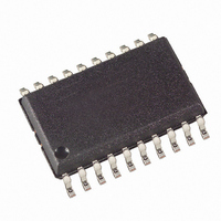
ATTINY861-20SU Atmel, ATTINY861-20SU Datasheet - Page 91

ATTINY861-20SU
Manufacturer Part Number
ATTINY861-20SU
Description
IC MCU AVR 8K FLASH 20MHZ 20SOIC
Manufacturer
Atmel
Series
AVR® ATtinyr
Datasheet
1.ATAVRMC321.pdf
(242 pages)
Specifications of ATTINY861-20SU
Core Processor
AVR
Core Size
8-Bit
Speed
20MHz
Connectivity
USI
Peripherals
Brown-out Detect/Reset, POR, PWM, WDT
Number Of I /o
16
Program Memory Size
8KB (4K x 16)
Program Memory Type
FLASH
Eeprom Size
512 x 8
Ram Size
512 x 8
Voltage - Supply (vcc/vdd)
2.7 V ~ 5.5 V
Data Converters
A/D 11x10b
Oscillator Type
Internal
Operating Temperature
-40°C ~ 85°C
Package / Case
20-SOIC (7.5mm Width)
Cpu Family
ATtiny
Device Core
AVR
Device Core Size
8b
Frequency (max)
20MHz
Interface Type
USI
Total Internal Ram Size
512Byte
# I/os (max)
16
Number Of Timers - General Purpose
2
Operating Supply Voltage (typ)
3.3/5V
Operating Supply Voltage (max)
5.5V
Operating Supply Voltage (min)
2.7V
On-chip Adc
11-chx10-bit
Instruction Set Architecture
RISC
Operating Temp Range
-40C to 85C
Operating Temperature Classification
Industrial
Mounting
Surface Mount
Pin Count
20
Package Type
SOIC
Processor Series
ATTINY8x
Core
AVR8
Data Bus Width
8 bit
Data Ram Size
512 B
Maximum Clock Frequency
20 MHz
Number Of Programmable I/os
16
Number Of Timers
2
Operating Supply Voltage
2.7 V to 5.5 V
Maximum Operating Temperature
+ 85 C
Mounting Style
SMD/SMT
3rd Party Development Tools
EWAVR, EWAVR-BL
Development Tools By Supplier
ATAVRDRAGON, ATSTK500, ATSTK600, ATAVRISP2, ATAVRONEKIT, ATAVRMC320
Minimum Operating Temperature
- 40 C
For Use With
ATSTK600 - DEV KIT FOR AVR/AVR32ATAVRBC100 - REF DESIGN KIT BATTERY CHARGER770-1007 - ISP 4PORT ATMEL AVR MCU SPI/JTAG770-1004 - ISP 4PORT FOR ATMEL AVR MCU SPI
Lead Free Status / RoHS Status
Lead free / RoHS Compliant
Available stocks
Company
Part Number
Manufacturer
Quantity
Price
- Current page: 91 of 242
- Download datasheet (5Mb)
12.2.5
2588E–AVR–08/10
Definitions
TCCR1A, TCCR1B, TCCR1C, TCCR1D, OCR1A, OCR1B, OCR1C and OCR1D can be read
back right after writing the register. The read back values are delayed for the Timer/Counter1
(TCNT1) register, Timer/Counter1 High Byte Register (TC1H) and flags (OCF1A, OCF1B,
OCF1D and TOV1), because of the input and output synchronization.
The system clock frequency must be lower than half of the PCK frequency, because the syn-
chronization mechanism of the asynchronous Timer/Counter1 needs at least two edges of the
PCK when the system clock is high. If the frequency of the system clock is too high, it is a risk
that data or control values are lost.
Figure 12-2. Timer/Counter1 Synchronization Register Block Diagram.
Many register and bit references in this section are written in general form. A lower case “n”
replaces the Timer/Counter number, in this case 0. A lower case “x” replaces the Output Com-
pare Unit, in this case Compare Unit A, B, C or D. However, when using the register or bit
defines in a program, the precise form must be used, i.e., TCNT1 for accessing Timer/Counter1
PCKE
CK
PCK
SYNC
MODE
ASYNC
MODE
IO-registers
OCR1B
OCF1A
OCR1A
OCR1C
OCR1D
TCCR1A
TCCR1B
TCCR1C
TCCR1D
TCNT1
TC1H
OCF1B
OCF1D
TOV1
~1/2 CK Delay
1/2 CK Delay
S
A
Input synchronization
registers
OCR1A_SI
OCR1B_SI
OCR1C_SI
OCR1D_SI
TCCR1A_SI
TCCR1B_SI
TCCR1C_SI
TCCR1D_SI
TCNT1_SI
TC1H_SI
OCF1A_SI
OCF1B_SI
OCF1D_SI
TOV1_SI
1 PCK Delay
1 CK Delay
S
A
8-BIT DATABUS
Timer/Counter1
TCNT1
1 CK Delay
1 PCK Delay
Output synchronization
registers
TCNT1_SO
TC1H_SO
OCF1A_SO
OCF1B_SO
OCF1D_SO
TOV1_SO
1/2 CK Delay
~1 CK Delay
TCNT1
TC1H
OCF1A
OCF1B
OCF1D
TOV1
91
Related parts for ATTINY861-20SU
Image
Part Number
Description
Manufacturer
Datasheet
Request
R

Part Number:
Description:
Manufacturer:
Atmel Corporation
Datasheet:

Part Number:
Description:
Manufacturer:
Atmel Corporation
Datasheet:

Part Number:
Description:
IC MCU AVR 8K FLASH 20MHZ 32-QFN
Manufacturer:
Atmel
Datasheet:

Part Number:
Description:
MCU AVR 8K FLASH 15MHZ 32-QFN
Manufacturer:
Atmel
Datasheet:

Part Number:
Description:
MCU AVR 8K FLASH 15MHZ 20-SOIC
Manufacturer:
Atmel
Datasheet:

Part Number:
Description:
MCU AVR 8KB FLASH 15MHZ 32-VQFN
Manufacturer:
Atmel
Datasheet:

Part Number:
Description:
Microcontrollers (MCU) 8kB Flash 0.512kB EEPROM 16 I/O Pins
Manufacturer:
Atmel
Datasheet:

Part Number:
Description:
8-bit Microcontrollers - MCU 8KB FL 512B EE 512B SRAM 20MHZ IND 5V
Manufacturer:
Atmel

Part Number:
Description:
IC, MCU, 8BIT, 2K FLASH, 20SOIC
Manufacturer:
Atmel
Datasheet:

Part Number:
Description:
IC, MCU, 8BIT, 2K FLASH, 20PDIP
Manufacturer:
Atmel
Datasheet:


