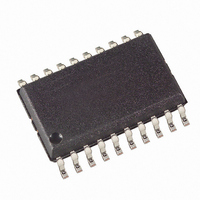
ATTINY861-20SU Atmel, ATTINY861-20SU Datasheet - Page 137

ATTINY861-20SU
Manufacturer Part Number
ATTINY861-20SU
Description
IC MCU AVR 8K FLASH 20MHZ 20SOIC
Manufacturer
Atmel
Series
AVR® ATtinyr
Datasheet
1.ATAVRMC321.pdf
(242 pages)
Specifications of ATTINY861-20SU
Core Processor
AVR
Core Size
8-Bit
Speed
20MHz
Connectivity
USI
Peripherals
Brown-out Detect/Reset, POR, PWM, WDT
Number Of I /o
16
Program Memory Size
8KB (4K x 16)
Program Memory Type
FLASH
Eeprom Size
512 x 8
Ram Size
512 x 8
Voltage - Supply (vcc/vdd)
2.7 V ~ 5.5 V
Data Converters
A/D 11x10b
Oscillator Type
Internal
Operating Temperature
-40°C ~ 85°C
Package / Case
20-SOIC (7.5mm Width)
Cpu Family
ATtiny
Device Core
AVR
Device Core Size
8b
Frequency (max)
20MHz
Interface Type
USI
Total Internal Ram Size
512Byte
# I/os (max)
16
Number Of Timers - General Purpose
2
Operating Supply Voltage (typ)
3.3/5V
Operating Supply Voltage (max)
5.5V
Operating Supply Voltage (min)
2.7V
On-chip Adc
11-chx10-bit
Instruction Set Architecture
RISC
Operating Temp Range
-40C to 85C
Operating Temperature Classification
Industrial
Mounting
Surface Mount
Pin Count
20
Package Type
SOIC
Processor Series
ATTINY8x
Core
AVR8
Data Bus Width
8 bit
Data Ram Size
512 B
Maximum Clock Frequency
20 MHz
Number Of Programmable I/os
16
Number Of Timers
2
Operating Supply Voltage
2.7 V to 5.5 V
Maximum Operating Temperature
+ 85 C
Mounting Style
SMD/SMT
3rd Party Development Tools
EWAVR, EWAVR-BL
Development Tools By Supplier
ATAVRDRAGON, ATSTK500, ATSTK600, ATAVRISP2, ATAVRONEKIT, ATAVRMC320
Minimum Operating Temperature
- 40 C
For Use With
ATSTK600 - DEV KIT FOR AVR/AVR32ATAVRBC100 - REF DESIGN KIT BATTERY CHARGER770-1007 - ISP 4PORT ATMEL AVR MCU SPI/JTAG770-1004 - ISP 4PORT FOR ATMEL AVR MCU SPI
Lead Free Status / RoHS Status
Lead free / RoHS Compliant
Available stocks
Company
Part Number
Manufacturer
Quantity
Price
- Current page: 137 of 242
- Download datasheet (5Mb)
14. AC – Analog Comparator
14.1
2588E–AVR–08/10
Analog Comparator Multiplexed Input
The analog comparator compares the input values on the selectable positive pin (AIN0, AIN1 or
AIN2) and selectable negative pin (AIN0, AIN1 or AIN2). When the voltage on the positive pin is
higher than the voltage on the negative pin, the Analog Comparator Output, ACO, is set. The
comparator can trigger a separate interrupt, exclusive to the analog comparator. The user can
select Interrupt triggering on comparator output rise, fall or toggle. A block diagram of the com-
parator and its surrounding logic is shown in
Figure 14-1. Analog Comparator Block Diagram
Notes:
See
When the Analog to Digital Converter (ADC) is configurated as single ended input channel, it is
possible to select any of the ADC10:0 pins to replace the negative input to the analog compara-
tor. The ADC multiplexer is used to select this input, and consequently, the ADC must be
switched off to utilize this feature. If the Analog Comparator Multiplexer Enable bit (ACME in
ADCSRB) is set and the ADC is switched off (ADEN in ADCSRA is zero), MUX5:0 in ADMUX
select the input pin to replace the negative input to the analog comparator, as shown in
14-1. If ACME is cleared or ADEN is set, either AIN0, AIN1 or AIN2 is applied to the negative
input to the analog comparator.
Table 14-1.
ACME
0
0
0
0
AIN0
AIN1
AIN2
Figure 1-1 on page 2
ADC MULTIPLEXER
1. See
ACM2..1
REFERENCE
ACME
ADEN
BANDGAP
OUTPUT
ADEN
x
x
x
x
Analog Comparator Multiplexed Input
Table 14-1 on page
MUX
(1)
ACBG
and
MUX5:0
xxxxxx
xxxxxx
xxxxxx
xxxxxx
Table 10-3 on page 63
137.
ACM2:0
000
001
010
011
Figure
14-1.
for Analog Comparator pin placement.
Positive Input
AIN0
AIN0
AIN1
AIN1
Negative Input
AIN1
AIN2
AIN0
AIN2
Table
137
Related parts for ATTINY861-20SU
Image
Part Number
Description
Manufacturer
Datasheet
Request
R

Part Number:
Description:
Manufacturer:
Atmel Corporation
Datasheet:

Part Number:
Description:
Manufacturer:
Atmel Corporation
Datasheet:

Part Number:
Description:
IC MCU AVR 8K FLASH 20MHZ 32-QFN
Manufacturer:
Atmel
Datasheet:

Part Number:
Description:
MCU AVR 8K FLASH 15MHZ 32-QFN
Manufacturer:
Atmel
Datasheet:

Part Number:
Description:
MCU AVR 8K FLASH 15MHZ 20-SOIC
Manufacturer:
Atmel
Datasheet:

Part Number:
Description:
MCU AVR 8KB FLASH 15MHZ 32-VQFN
Manufacturer:
Atmel
Datasheet:

Part Number:
Description:
Microcontrollers (MCU) 8kB Flash 0.512kB EEPROM 16 I/O Pins
Manufacturer:
Atmel
Datasheet:

Part Number:
Description:
8-bit Microcontrollers - MCU 8KB FL 512B EE 512B SRAM 20MHZ IND 5V
Manufacturer:
Atmel

Part Number:
Description:
IC, MCU, 8BIT, 2K FLASH, 20SOIC
Manufacturer:
Atmel
Datasheet:

Part Number:
Description:
IC, MCU, 8BIT, 2K FLASH, 20PDIP
Manufacturer:
Atmel
Datasheet:


