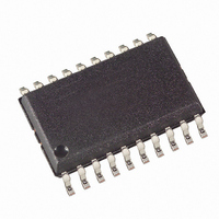
ATTINY861-20SU Atmel, ATTINY861-20SU Datasheet - Page 149

ATTINY861-20SU
Manufacturer Part Number
ATTINY861-20SU
Description
IC MCU AVR 8K FLASH 20MHZ 20SOIC
Manufacturer
Atmel
Series
AVR® ATtinyr
Datasheet
1.ATAVRMC321.pdf
(242 pages)
Specifications of ATTINY861-20SU
Core Processor
AVR
Core Size
8-Bit
Speed
20MHz
Connectivity
USI
Peripherals
Brown-out Detect/Reset, POR, PWM, WDT
Number Of I /o
16
Program Memory Size
8KB (4K x 16)
Program Memory Type
FLASH
Eeprom Size
512 x 8
Ram Size
512 x 8
Voltage - Supply (vcc/vdd)
2.7 V ~ 5.5 V
Data Converters
A/D 11x10b
Oscillator Type
Internal
Operating Temperature
-40°C ~ 85°C
Package / Case
20-SOIC (7.5mm Width)
Cpu Family
ATtiny
Device Core
AVR
Device Core Size
8b
Frequency (max)
20MHz
Interface Type
USI
Total Internal Ram Size
512Byte
# I/os (max)
16
Number Of Timers - General Purpose
2
Operating Supply Voltage (typ)
3.3/5V
Operating Supply Voltage (max)
5.5V
Operating Supply Voltage (min)
2.7V
On-chip Adc
11-chx10-bit
Instruction Set Architecture
RISC
Operating Temp Range
-40C to 85C
Operating Temperature Classification
Industrial
Mounting
Surface Mount
Pin Count
20
Package Type
SOIC
Processor Series
ATTINY8x
Core
AVR8
Data Bus Width
8 bit
Data Ram Size
512 B
Maximum Clock Frequency
20 MHz
Number Of Programmable I/os
16
Number Of Timers
2
Operating Supply Voltage
2.7 V to 5.5 V
Maximum Operating Temperature
+ 85 C
Mounting Style
SMD/SMT
3rd Party Development Tools
EWAVR, EWAVR-BL
Development Tools By Supplier
ATAVRDRAGON, ATSTK500, ATSTK600, ATAVRISP2, ATAVRONEKIT, ATAVRMC320
Minimum Operating Temperature
- 40 C
For Use With
ATSTK600 - DEV KIT FOR AVR/AVR32ATAVRBC100 - REF DESIGN KIT BATTERY CHARGER770-1007 - ISP 4PORT ATMEL AVR MCU SPI/JTAG770-1004 - ISP 4PORT FOR ATMEL AVR MCU SPI
Lead Free Status / RoHS Status
Lead free / RoHS Compliant
Available stocks
Company
Part Number
Manufacturer
Quantity
Price
15.6.1
15.6.2
15.7
2588E–AVR–08/10
ADC Noise Canceler
ADC Input Channels
ADC Voltage Reference
When updating ADMUX in one of these conditions, the new settings will affect the next ADC
conversion.
When changing channel selections, the user should observe the following guidelines to ensure
that the correct channel is selected:
In Single Conversion mode, always select the channel before starting the conversion. The chan-
nel selection may be changed one ADC clock cycle after writing one to ADSC. However, the
simplest method is to wait for the conversion to complete before changing the channel selection.
In Free Running mode, always select the channel before starting the first conversion. The chan-
nel selection may be changed one ADC clock cycle after writing one to ADSC. However, the
simplest method is to wait for the first conversion to complete, and then change the channel
selection. Since the next conversion has already started automatically, the next result will reflect
the previous channel selection. Subsequent conversions will reflect the new channel selection.
The voltage reference for the ADC (V
ended channels that exceed V
either V
version result after switching voltage reference source may be inaccurate, and the user is
advised to discard this result.
The ADC features a noise canceler that enables conversion during sleep mode. This reduces
noise induced from the CPU core and other I/O peripherals. The noise canceler can be used
with ADC Noise Reduction and Idle mode. To make use of this feature, the following procedure
should be used:
Note that the ADC will not automatically be turned off when entering other sleep modes than Idle
mode and ADC Noise Reduction mode. The user is advised to write zero to ADEN before enter-
ing such sleep modes to avoid excessive power consumption.
• When ADATE or ADEN is cleared.
• During conversion, minimum one ADC clock cycle after the trigger event.
• After a conversion, before the Interrupt Flag used as trigger source is cleared.
• Make sure that the ADC is enabled and is not busy converting. Single Conversion mode must
• Enter ADC Noise Reduction mode (or Idle mode). The ADC will start a conversion once the
• If no other interrupts occur before the ADC conversion completes, the ADC interrupt will
be selected and the ADC conversion complete interrupt must be enabled.
CPU has been halted.
wake up the CPU and execute the ADC Conversion Complete interrupt routine. If another
interrupt wakes up the CPU before the ADC conversion is complete, that interrupt will be
executed, and an ADC Conversion Complete interrupt request will be generated when the
ADC conversion completes. The CPU will remain in active mode until a new sleep command
is executed.
CC
, or internal 1.1V / 2.56V voltage reference, or external AREF pin. The first ADC con-
REF
will result in codes close to 0x3FF. V
REF
) indicates the conversion range for the ADC. Single
REF
can be selected as
149


