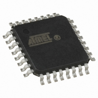
ATMEGA16U2-AUR Atmel, ATMEGA16U2-AUR Datasheet - Page 206

ATMEGA16U2-AUR
Manufacturer Part Number
ATMEGA16U2-AUR
Description
MCU AVR 8K FLASH 16MHZ 32TQFP
Manufacturer
Atmel
Series
AVR® ATmegar
Specifications of ATMEGA16U2-AUR
Core Processor
AVR
Core Size
8-Bit
Speed
16MHz
Connectivity
SPI, UART/USART, USB
Peripherals
Brown-out Detect/Reset, POR, PWM, WDT
Number Of I /o
22
Program Memory Size
16KB (8K x 16)
Program Memory Type
FLASH
Eeprom Size
512 x 8
Ram Size
512 x 8
Voltage - Supply (vcc/vdd)
2.7 V ~ 5.5 V
Oscillator Type
Internal
Operating Temperature
-40°C ~ 85°C
Package / Case
32-TQFP, 32-VQFP
Lead Free Status / RoHS Status
Lead free / RoHS Compliant
Data Converters
-
- Current page: 206 of 309
- Download datasheet (6Mb)
21.14.1
21.14.1.1
7799D–AVR–11/10
Example with 1 IN data bank
Detailed description
Example with 2 IN data banks
FIFOCON
FIFOCON
TXINI
TXINI
Abort
SW
SW
write data from CPU
write data from CPU
The RWAL bit always reflects the state of the current bank. This bit is set if the firmware can
write data to the bank, and cleared by hardware when the bank is full.
The data are written by the CPU, following the next flow:
If the endpoint uses 2 banks, the second one can be read by the HOST while the current is
being written by the CPU. Then, when the CPU clears FIFOCON, the next bank may be already
ready (free) and TXINI is set immediately.
An “abort” stage can be produced by the host in some situations:
• When the bank is empty, an endpoint interrupt (EPINTx) is triggered, if enabled (TXINE set)
• The CPU acknowledges the interrupt by clearing TXINI,
• The CPU can write the data into the current bank (write in UEDATX),
• The CPU can free the bank by clearing FIFOCON when all the data are written, that is:
• after “N” write into UEDATX
• as soon as RWAL is cleared by hardware.
NAK
BANK 0
and TXINI is set. The CPU can also poll TXINI or FIFOCON, depending the software
architecture choice,
BANK 0
SW
SW
IN
IN
SW
write data from CPU
BANK 1
(bank 0)
(bank 0)
DATA
DATA
SW
HW
HW
ACK
ACK
ATmega8U2/16U2/32U2
SW
SW
write data from CPU
write data from CPU
IN
BANK 0
BANK0
(bank 1)
DATA
SW
IN
ACK
206
Related parts for ATMEGA16U2-AUR
Image
Part Number
Description
Manufacturer
Datasheet
Request
R

Part Number:
Description:
Manufacturer:
Atmel Corporation
Datasheet:

Part Number:
Description:
IC AVR MCU 16K 16MHZ 5V 44TQFP
Manufacturer:
Atmel
Datasheet:

Part Number:
Description:
IC AVR MCU 16K 16MHZ 5V 44-QFN
Manufacturer:
Atmel
Datasheet:

Part Number:
Description:
IC AVR MCU 16K 16MHZ 5V 40DIP
Manufacturer:
Atmel
Datasheet:

Part Number:
Description:
MCU AVR 16K FLASH 16MHZ 44-QFN
Manufacturer:
Atmel
Datasheet:

Part Number:
Description:
IC AVR MCU 16K 16MHZ COM 40-DIP
Manufacturer:
Atmel
Datasheet:

Part Number:
Description:
IC AVR MCU 16K 16MHZ COM 44-QFN
Manufacturer:
Atmel
Datasheet:

Part Number:
Description:
IC AVR MCU 16K 16MHZ IND 40-DIP
Manufacturer:
Atmel
Datasheet:

Part Number:
Description:
IC AVR MCU 16K 16MHZ IND 44-QFN
Manufacturer:
Atmel
Datasheet:

Part Number:
Description:
IC AVR MCU 16K 16MHZ IND 44-TQFP
Manufacturer:
Atmel
Datasheet:

Part Number:
Description:
IC MCU 8BIT 16KB FLASH 44TQFP
Manufacturer:
Atmel
Datasheet:

Part Number:
Description:
MCU AVR 16K FLASH 16MHZ 44-TQFP
Manufacturer:
Atmel
Datasheet:

Part Number:
Description:
IC AVR MCU 16K 16MHZ COM 44-TQFP
Manufacturer:
Atmel
Datasheet:


