PIC16LF1826-I/MV Microchip Technology, PIC16LF1826-I/MV Datasheet - Page 286
PIC16LF1826-I/MV
Manufacturer Part Number
PIC16LF1826-I/MV
Description
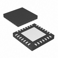
IC MCU 8BIT FLASH 28UQFN
Manufacturer
Microchip Technology
Series
PIC® XLP™ 16Fr
Datasheet
1.PIC16F1826-IP.pdf
(406 pages)
Specifications of PIC16LF1826-I/MV
Core Size
8-Bit
Program Memory Size
3.5KB (2K x 14)
Core Processor
PIC
Speed
32MHz
Connectivity
I²C, SPI, UART/USART
Peripherals
Brown-out Detect/Reset, POR, PWM, WDT
Number Of I /o
16
Program Memory Type
FLASH
Eeprom Size
256 x 8
Ram Size
256 x 8
Voltage - Supply (vcc/vdd)
1.8 V ~ 3.6 V
Data Converters
A/D 12x10b
Oscillator Type
Internal
Operating Temperature
-40°C ~ 85°C
Package / Case
28-UFQFN Exposed Pad
Controller Family/series
PIC16LF
No. Of I/o's
16
Eeprom Memory Size
256Byte
Ram Memory Size
256Byte
Cpu Speed
32MHz
No. Of Timers
3
Processor Series
PIC16LF
Core
PIC
Data Ram Size
256 B
Maximum Clock Frequency
32 KHz
Number Of Programmable I/os
16
Number Of Timers
3
Operating Supply Voltage
1.8 V to 3.6 V
Maximum Operating Temperature
+ 125 C
3rd Party Development Tools
52715-96, 52716-328, 52717-734
Development Tools By Supplier
PG164130, DV164035, DV244005, DV164005
Minimum Operating Temperature
- 40 C
On-chip Adc
10 bit, 12 Channel
On-chip Dac
5 bit
Lead Free Status / RoHS Status
Lead free / RoHS Compliant
Lead Free Status / RoHS Status
Lead free / RoHS Compliant


PIC16F/LF1826/27
REGISTER 24-5:
REGISTER 24-6:
DS41391C-page 286
bit 7
Legend:
R = Readable bit
u = Bit is unchanged
‘1’ = Bit is set
bit 7-1
bit 0
bit 7
Legend:
R = Readable bit
u = Bit is unchanged
‘1’ = Bit is set
Master mode:
bit 7-0
10-Bit Slave mode — Most Significant Address byte:
bit 7-3
bit 2-1
bit 0
10-Bit Slave mode — Least Significant Address byte:
bit 7-0
7-Bit Slave mode:
bit 7-1
bit 0
R/W-1/1
R/W-0/0
ADD<7:0>: Baud Rate Clock Divider bits
SCLx pin clock period = ((ADD<7:0> + 1) *4)/F
Not used: Unused for Most Significant Address byte. Bit state of this register is a “don’t care”. Bit pat-
tern sent by master is fixed by I
compared by hardware and are not affected by the value in this register.
ADD<2:1>: Two Most Significant bits of 10-bit address
Not used: Unused in this mode. Bit state is a “don’t care”.
ADD<7:0>: Eight Least Significant bits of 10-bit address
ADD<7:1>: 7-bit address
Not used: Unused in this mode. Bit state is a “don’t care”.
MSK<7:1>: Mask bits
1 = The received address bit n is compared to SSPxADD<n> to detect I
0 = The received address bit n is not used to detect I
MSK<0>: Mask bit for I
I
1 = The received address bit 0 is compared to SSPxADD<0> to detect I
0 = The received address bit 0 is not used to detect I
I
2
2
C Slave mode, 10-bit address (SSPxM<3:0> = 0111 or 1111):
C Slave mode, 7-bit address, the bit is ignored
R/W-0/0
R/W-1/1
SSPxMSK: SSPx MASK REGISTER
SSPxADD: MSSPx ADDRESS AND BAUD RATE REGISTER (I
W = Writable bit
x = Bit is unknown
‘0’ = Bit is cleared
W = Writable bit
x = Bit is unknown
‘0’ = Bit is cleared
R/W-0/0
R/W-1/1
2
C Slave mode, 10-bit Address
2
C specification and must be equal to ‘11110’. However, those bits are
R/W-1/1
R/W-0/0
Preliminary
ADD<7:0>
MSK<7:0>
U = Unimplemented bit, read as ‘0’
-n/n = Value at POR and BOR/Value at all other Resets
U = Unimplemented bit, read as ‘0’
-n/n = Value at POR and BOR/Value at all other Resets
R/W-1/1
R/W-0/0
OSC
2
2
C address match
C address match
R/W-1/1
R/W-0/0
2010 Microchip Technology Inc.
2
2
C address match
C address match
R/W-0/0
R/W-1/1
2
C MODE)
R/W-0/0
R/W-1/1
bit 0
bit 0
Related parts for PIC16LF1826-I/MV
Image
Part Number
Description
Manufacturer
Datasheet
Request
R

Part Number:
Description:
IC, 8BIT MCU, PIC16LF, 32MHZ, QFN-28
Manufacturer:
Microchip Technology
Datasheet:

Part Number:
Description:
IC, 8BIT MCU, PIC16LF, 32MHZ, QFN-28
Manufacturer:
Microchip Technology
Datasheet:

Part Number:
Description:
IC, 8BIT MCU, PIC16LF, 32MHZ, DIP-18
Manufacturer:
Microchip Technology
Datasheet:

Part Number:
Description:
IC, 8BIT MCU, PIC16LF, 20MHZ, TQFP-44
Manufacturer:
Microchip Technology
Datasheet:
Part Number:
Description:
7 KB Flash, 384 Bytes RAM, 32 MHz Int. Osc, 16 I/0, Enhanced Mid Range Core, Nan
Manufacturer:
Microchip Technology

Part Number:
Description:
14KB Flash, 512B RAM, LCD, 11x10b ADC, EUSART, NanoWatt XLP 28 SOIC .300in T/R
Manufacturer:
Microchip Technology
Datasheet:
Part Number:
Description:
14KB Flash, 512B RAM, LCD, 11x10b ADC, EUSART, NanoWatt XLP 28 SSOP .209in T/R
Manufacturer:
Microchip Technology
Datasheet:
Part Number:
Description:
MCU PIC 14KB FLASH XLP 28-SSOP
Manufacturer:
Microchip Technology
Part Number:
Description:
MCU PIC 14KB FLASH XLP 28-SOIC
Manufacturer:
Microchip Technology
Part Number:
Description:
MCU PIC 512B FLASH XLP 28-UQFN
Manufacturer:
Microchip Technology
Part Number:
Description:
MCU PIC 14KB FLASH XLP 28-SPDIP
Manufacturer:
Microchip Technology

Part Number:
Description:
MCU 7KB FLASH 256B RAM 40-UQFN
Manufacturer:
Microchip Technology
Part Number:
Description:
MCU 7KB FLASH 256B RAM 44-TQFP
Manufacturer:
Microchip Technology

Part Number:
Description:
MCU 14KB FLASH 1KB RAM 28-UQFN
Manufacturer:
Microchip Technology
Part Number:
Description:
MCU PIC 14KB FLASH XLP 40-UQFN
Manufacturer:
Microchip Technology