PIC16LF1826-I/MV Microchip Technology, PIC16LF1826-I/MV Datasheet - Page 140
PIC16LF1826-I/MV
Manufacturer Part Number
PIC16LF1826-I/MV
Description
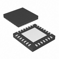
IC MCU 8BIT FLASH 28UQFN
Manufacturer
Microchip Technology
Series
PIC® XLP™ 16Fr
Datasheet
1.PIC16F1826-IP.pdf
(406 pages)
Specifications of PIC16LF1826-I/MV
Core Size
8-Bit
Program Memory Size
3.5KB (2K x 14)
Core Processor
PIC
Speed
32MHz
Connectivity
I²C, SPI, UART/USART
Peripherals
Brown-out Detect/Reset, POR, PWM, WDT
Number Of I /o
16
Program Memory Type
FLASH
Eeprom Size
256 x 8
Ram Size
256 x 8
Voltage - Supply (vcc/vdd)
1.8 V ~ 3.6 V
Data Converters
A/D 12x10b
Oscillator Type
Internal
Operating Temperature
-40°C ~ 85°C
Package / Case
28-UFQFN Exposed Pad
Controller Family/series
PIC16LF
No. Of I/o's
16
Eeprom Memory Size
256Byte
Ram Memory Size
256Byte
Cpu Speed
32MHz
No. Of Timers
3
Processor Series
PIC16LF
Core
PIC
Data Ram Size
256 B
Maximum Clock Frequency
32 KHz
Number Of Programmable I/os
16
Number Of Timers
3
Operating Supply Voltage
1.8 V to 3.6 V
Maximum Operating Temperature
+ 125 C
3rd Party Development Tools
52715-96, 52716-328, 52717-734
Development Tools By Supplier
PG164130, DV164035, DV244005, DV164005
Minimum Operating Temperature
- 40 C
On-chip Adc
10 bit, 12 Channel
On-chip Dac
5 bit
Lead Free Status / RoHS Status
Lead free / RoHS Compliant
Lead Free Status / RoHS Status
Lead free / RoHS Compliant


PIC16F/LF1826/27
15.1
When configuring and using the ADC the following
functions must be considered:
• Port configuration
• Channel selection
• ADC voltage reference selection
• ADC conversion clock source
• Interrupt control
• Result formatting
15.1.1
The ADC can be used to convert both analog and
digital signals. When converting analog signals, the I/O
pin should be configured for analog by setting the
associated
Section 12.0 “I/O Ports” for more information.
15.1.2
There are up to 14 channel selections available:
• AN<11:0> pins
• DAC Output
• FVR (Fixed Voltage Reference) Output
Refer to Section 16.0 “Digital-to-Analog Converter
(DAC) Module” and Section 14.0 “Fixed Voltage
Reference (FVR)” for more information on these
channel selections.
The CHS bits of the ADCON0 register determine which
channel is connected to the sample and hold circuit.
When changing channels, a delay is required before
starting the next conversion. Refer to Section 15.2
“ADC Operation” for more information.
15.1.3
The ADPREF bits of the ADCON1 register provides
control of the positive voltage reference. The positive
voltage reference can be:
• V
• V
• FVR 2.028V
• FVR 4.096V (Not available on LF devices)
The ADNREF bits of the ADCON1 register provides
control of the negative voltage reference. The negative
voltage reference can be:
• V
• V
See Section 14.0 “Fixed Voltage Reference (FVR)”
for more details on the fixed voltage reference.
DS41391C-page 140
Note:
REF
DD
REF
SS
+ pin
- pin
ADC Configuration
PORT CONFIGURATION
Analog voltages on any pin that is defined
as a digital input may cause the input buf-
fer to conduct excess current.
CHANNEL SELECTION
ADC VOLTAGE REFERENCE
TRIS
and
ANSEL
bits.
Refer
Preliminary
to
15.1.4
The source of the conversion clock is software select-
able via the ADCS bits of the ADCON1 register. There
are seven possible clock options:
• F
• F
• F
• F
• F
• F
• F
The time to complete one bit conversion is defined as
T
ods as shown in Figure 15-2.
For correct conversion, the appropriate T
must be met. Refer to the A/D conversion requirements
in Section 29.0 “Electrical Specifications” for more
information. Table 15-1 gives examples of appropriate
ADC clock selections.
AD
Note:
OSC
OSC
OSC
OSC
OSC
OSC
RC
. One full 10-bit conversion requires 11.5 T
(dedicated internal oscillator)
/2
/4
/8
/16
/32
/64
CONVERSION CLOCK
Unless using the F
system clock frequency will change the
ADC
adversely affect the ADC result.
clock
2010 Microchip Technology Inc.
frequency,
RC
, any changes in the
AD
which
specification
AD
may
peri-
Related parts for PIC16LF1826-I/MV
Image
Part Number
Description
Manufacturer
Datasheet
Request
R

Part Number:
Description:
IC, 8BIT MCU, PIC16LF, 32MHZ, QFN-28
Manufacturer:
Microchip Technology
Datasheet:

Part Number:
Description:
IC, 8BIT MCU, PIC16LF, 32MHZ, QFN-28
Manufacturer:
Microchip Technology
Datasheet:

Part Number:
Description:
IC, 8BIT MCU, PIC16LF, 32MHZ, DIP-18
Manufacturer:
Microchip Technology
Datasheet:

Part Number:
Description:
IC, 8BIT MCU, PIC16LF, 20MHZ, TQFP-44
Manufacturer:
Microchip Technology
Datasheet:
Part Number:
Description:
7 KB Flash, 384 Bytes RAM, 32 MHz Int. Osc, 16 I/0, Enhanced Mid Range Core, Nan
Manufacturer:
Microchip Technology

Part Number:
Description:
14KB Flash, 512B RAM, LCD, 11x10b ADC, EUSART, NanoWatt XLP 28 SOIC .300in T/R
Manufacturer:
Microchip Technology
Datasheet:
Part Number:
Description:
14KB Flash, 512B RAM, LCD, 11x10b ADC, EUSART, NanoWatt XLP 28 SSOP .209in T/R
Manufacturer:
Microchip Technology
Datasheet:
Part Number:
Description:
MCU PIC 14KB FLASH XLP 28-SSOP
Manufacturer:
Microchip Technology
Part Number:
Description:
MCU PIC 14KB FLASH XLP 28-SOIC
Manufacturer:
Microchip Technology
Part Number:
Description:
MCU PIC 512B FLASH XLP 28-UQFN
Manufacturer:
Microchip Technology
Part Number:
Description:
MCU PIC 14KB FLASH XLP 28-SPDIP
Manufacturer:
Microchip Technology

Part Number:
Description:
MCU 7KB FLASH 256B RAM 40-UQFN
Manufacturer:
Microchip Technology
Part Number:
Description:
MCU 7KB FLASH 256B RAM 44-TQFP
Manufacturer:
Microchip Technology

Part Number:
Description:
MCU 14KB FLASH 1KB RAM 28-UQFN
Manufacturer:
Microchip Technology
Part Number:
Description:
MCU PIC 14KB FLASH XLP 40-UQFN
Manufacturer:
Microchip Technology