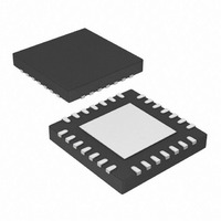
PIC16LF1826-I/MV Microchip Technology, PIC16LF1826-I/MV Datasheet - Page 213

PIC16LF1826-I/MV
Manufacturer Part Number
PIC16LF1826-I/MV
Description
IC MCU 8BIT FLASH 28UQFN
Manufacturer
Microchip Technology
Series
PIC® XLP™ 16Fr
Datasheet
1.PIC16F1826-IP.pdf
(406 pages)
Specifications of PIC16LF1826-I/MV
Core Size
8-Bit
Program Memory Size
3.5KB (2K x 14)
Core Processor
PIC
Speed
32MHz
Connectivity
I²C, SPI, UART/USART
Peripherals
Brown-out Detect/Reset, POR, PWM, WDT
Number Of I /o
16
Program Memory Type
FLASH
Eeprom Size
256 x 8
Ram Size
256 x 8
Voltage - Supply (vcc/vdd)
1.8 V ~ 3.6 V
Data Converters
A/D 12x10b
Oscillator Type
Internal
Operating Temperature
-40°C ~ 85°C
Package / Case
28-UFQFN Exposed Pad
Controller Family/series
PIC16LF
No. Of I/o's
16
Eeprom Memory Size
256Byte
Ram Memory Size
256Byte
Cpu Speed
32MHz
No. Of Timers
3
Processor Series
PIC16LF
Core
PIC
Data Ram Size
256 B
Maximum Clock Frequency
32 KHz
Number Of Programmable I/os
16
Number Of Timers
3
Operating Supply Voltage
1.8 V to 3.6 V
Maximum Operating Temperature
+ 125 C
3rd Party Development Tools
52715-96, 52716-328, 52717-734
Development Tools By Supplier
PG164130, DV164035, DV244005, DV164005
Minimum Operating Temperature
- 40 C
On-chip Adc
10 bit, 12 Channel
On-chip Dac
5 bit
Lead Free Status / RoHS Status
Lead free / RoHS Compliant
Lead Free Status / RoHS Status
Lead free / RoHS Compliant
- Current page: 213 of 406
- Download datasheet (4Mb)
23.3.7
In Sleep mode, the TMRx register will not increment
and the state of the module will not change. If the CCPx
pin is driving a value, it will continue to drive that value.
When the device wakes up, TMRx will continue from its
previous state.
23.3.8
The PWM frequency is derived from the system clock
frequency. Any changes in the system clock frequency
will result in changes to the PWM frequency. See
Section 5.0 “Oscillator Module (With Fail-Safe
Clock Monitor)” for additional details.
23.3.9
Any Reset will force all ports to Input mode and the
CCP registers to their Reset states.
TABLE 23-8:
2010 Microchip Technology Inc.
APFCON0
CCPxCON
CCPxAS
CCPTMRS
INTCON
PRx
PSTRxCON
PWMxCON
TxCON
TMRx
TRISB
Legend: — = Unimplemented locations, read as ‘0’. Shaded cells are not used by the PWM.
Note 1:
Name
2:
*
Page provides register information.
Applies to ECCP modules only.
PIC16F/LF1827 only.
OPERATION IN SLEEP MODE
CHANGES IN SYSTEM CLOCK
FREQUENCY
EFFECTS OF RESET
Timerx Period Register
Timerx Module Register
RXDTSEL
CCPxASE
C4TSEL1
PxRSEN
PxM1
TRISB7
Bit 7
GIE
—
—
SUMMARY OF REGISTERS ASSOCIATED WITH PWM
(1)
TxOUTPS3 TxOUTPS2 TxOUTPS1 TxOUTPS0
SDO1SEL
CCPxAS2
C4TSEL0
PxM0
TRISB6
PxDC6
PEIE
Bit 6
—
(1)
CCPxAS1
C3TSEL1
SS1SEL
TMR0IE
TRISB5
DCxB1
PxDC5
Bit 5
—
STRxSYNC
P2BSEL
CCPxAS0
C3TSEL0
TRISB4
DCxB0
PxDC4
Preliminary
INTE
Bit 4
(2)
CCP2SEL
PSSxAC1
C2TSEL1
CCPxM3
TRISB3
STRxD
PxDC3
IOCIE
23.3.10
This module incorporates I/O pins that can be moved to
other locations with the use of the alternate pin function
registers, APFCON0 and APFCON1. To determine
which pins can be moved and what their default loca-
tions are upon a Reset, see Section 12.1 “Alternate
Pin Function” for more information.
Bit 3
(2)
PIC16F/LF1826/27
PSSxAC0
C2TSEL0
TMRxON
CCPxM2
P1DSEL
TMR0IF
TRISB2
STRxC
PxDC2
ALTERNATE PIN LOCATIONS
Bit 2
PSSxBD1
C1TSEL1
TxCKPS1
CCPxM1
P1CSEL
TRISB1
STRxB
PxDC1
INTF
Bit 1
CCP1SEL
PSSxBD0
TxCKPS0
C1TSEL0
CCPxM0
TRISB0
STRxA
PxDC0
IOCIF
DS41391C-page 213
Bit 0
Register
on Page
191*
191*
122
228
230
229
232
231
193
129
91
Related parts for PIC16LF1826-I/MV
Image
Part Number
Description
Manufacturer
Datasheet
Request
R

Part Number:
Description:
IC, 8BIT MCU, PIC16LF, 32MHZ, QFN-28
Manufacturer:
Microchip Technology
Datasheet:

Part Number:
Description:
IC, 8BIT MCU, PIC16LF, 32MHZ, QFN-28
Manufacturer:
Microchip Technology
Datasheet:

Part Number:
Description:
IC, 8BIT MCU, PIC16LF, 32MHZ, DIP-18
Manufacturer:
Microchip Technology
Datasheet:

Part Number:
Description:
IC, 8BIT MCU, PIC16LF, 20MHZ, TQFP-44
Manufacturer:
Microchip Technology
Datasheet:

Part Number:
Description:
7 KB Flash, 384 Bytes RAM, 32 MHz Int. Osc, 16 I/0, Enhanced Mid Range Core, Nan
Manufacturer:
Microchip Technology

Part Number:
Description:
14KB Flash, 512B RAM, LCD, 11x10b ADC, EUSART, NanoWatt XLP 28 SOIC .300in T/R
Manufacturer:
Microchip Technology
Datasheet:

Part Number:
Description:
14KB Flash, 512B RAM, LCD, 11x10b ADC, EUSART, NanoWatt XLP 28 SSOP .209in T/R
Manufacturer:
Microchip Technology
Datasheet:

Part Number:
Description:
MCU PIC 14KB FLASH XLP 28-SSOP
Manufacturer:
Microchip Technology

Part Number:
Description:
MCU PIC 14KB FLASH XLP 28-SOIC
Manufacturer:
Microchip Technology

Part Number:
Description:
MCU PIC 512B FLASH XLP 28-UQFN
Manufacturer:
Microchip Technology

Part Number:
Description:
MCU PIC 14KB FLASH XLP 28-SPDIP
Manufacturer:
Microchip Technology

Part Number:
Description:
MCU 7KB FLASH 256B RAM 40-UQFN
Manufacturer:
Microchip Technology

Part Number:
Description:
MCU 7KB FLASH 256B RAM 44-TQFP
Manufacturer:
Microchip Technology

Part Number:
Description:
MCU 14KB FLASH 1KB RAM 28-UQFN
Manufacturer:
Microchip Technology

Part Number:
Description:
MCU PIC 14KB FLASH XLP 40-UQFN
Manufacturer:
Microchip Technology


