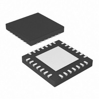
PIC16LF1826-I/MV Microchip Technology, PIC16LF1826-I/MV Datasheet - Page 120

PIC16LF1826-I/MV
Manufacturer Part Number
PIC16LF1826-I/MV
Description
IC MCU 8BIT FLASH 28UQFN
Manufacturer
Microchip Technology
Series
PIC® XLP™ 16Fr
Datasheet
1.PIC16F1826-IP.pdf
(406 pages)
Specifications of PIC16LF1826-I/MV
Core Size
8-Bit
Program Memory Size
3.5KB (2K x 14)
Core Processor
PIC
Speed
32MHz
Connectivity
I²C, SPI, UART/USART
Peripherals
Brown-out Detect/Reset, POR, PWM, WDT
Number Of I /o
16
Program Memory Type
FLASH
Eeprom Size
256 x 8
Ram Size
256 x 8
Voltage - Supply (vcc/vdd)
1.8 V ~ 3.6 V
Data Converters
A/D 12x10b
Oscillator Type
Internal
Operating Temperature
-40°C ~ 85°C
Package / Case
28-UFQFN Exposed Pad
Controller Family/series
PIC16LF
No. Of I/o's
16
Eeprom Memory Size
256Byte
Ram Memory Size
256Byte
Cpu Speed
32MHz
No. Of Timers
3
Processor Series
PIC16LF
Core
PIC
Data Ram Size
256 B
Maximum Clock Frequency
32 KHz
Number Of Programmable I/os
16
Number Of Timers
3
Operating Supply Voltage
1.8 V to 3.6 V
Maximum Operating Temperature
+ 125 C
3rd Party Development Tools
52715-96, 52716-328, 52717-734
Development Tools By Supplier
PG164130, DV164035, DV244005, DV164005
Minimum Operating Temperature
- 40 C
On-chip Adc
10 bit, 12 Channel
On-chip Dac
5 bit
Lead Free Status / RoHS Status
Lead free / RoHS Compliant
Lead Free Status / RoHS Status
Lead free / RoHS Compliant
- Current page: 120 of 406
- Download datasheet (4Mb)
PIC16F/LF1826/27
REGISTER 11-6:
TABLE 11-3:
DS41391C-page 120
EECON1
EECON2 EEPROM Control Register 2 (not a physical register)
EEADRL EEADRL7 EEADRL6 EEADRL5 EEADRL4 EEADRL3 EEADRL2 EEADRL1 EEADRL0
EEADRH
EEDATL
EEDATH
INTCON
PIE2
PIR2
Legend: — = unimplemented read as ‘0’. Shaded cells are not used by Data EEPROM module.
bit 7
Legend:
R = Readable bit
S = Bit can only be set
‘1’ = Bit is set
bit 7-0
Name
W-0/0
*
Page provides register information.
EEDATL7 EEDATL6 EEDATL5 EEDATL4 EEDATL3 EEDATL2 EEDALT1 EEDATL0
EEPGD
OSFIE
OSFIF
Bit 7
GIE
—
—
Data EEPROM Unlock Pattern bits
To unlock writes, a 55h must be written first, followed by an AAh, before setting the WR bit of the
EECON1 register. The value written to this register is used to unlock the writes. There are specific
timing requirements on these writes. Refer to Section 11.2.2 “Writing to the Data EEPROM
Memory” for more information.
SUMMARY OF REGISTERS ASSOCIATED WITH DATA EEPROM
W-0/0
EECON2: EEPROM CONTROL 2 REGISTER
EEADRH6 EEADRH5 EEADRH4 EEADRH3 EEADRH2 EEADRH1 EEADRH0
CFGS
PEIE
C2IE
Bit 6
C2IF
—
W = Writable bit
x = Bit is unknown
‘0’ = Bit is cleared
W-0/0
EEDATH5 EEDATH4 EEDATH3 EEDATH2 EEDATH1 EEDATH0
TMR0IE
LWLO
Bit 5
C1IE
C1IF
EEPROM Control Register 2
W-0/0
FREE
Bit 4
INTE
EEIE
EEIF
Preliminary
WRERR
U = Unimplemented bit, read as ‘0’
-n/n = Value at POR and BOR/Value at all other Resets
BCL1IE
BCL1IF
IOCIE
Bit 3
W-0/0
TMR0IF
WREN
Bit 2
—
—
W-0/0
Bit 1
INTF
WR
—
—
2010 Microchip Technology Inc.
W-0/0
CCP2IE
CCP2IF
IOCIF
Bit 0
RD
Register
on Page
W-0/0
107*
119
118
118
118
118
91
93
97
bit 0
Related parts for PIC16LF1826-I/MV
Image
Part Number
Description
Manufacturer
Datasheet
Request
R

Part Number:
Description:
IC, 8BIT MCU, PIC16LF, 32MHZ, QFN-28
Manufacturer:
Microchip Technology
Datasheet:

Part Number:
Description:
IC, 8BIT MCU, PIC16LF, 32MHZ, QFN-28
Manufacturer:
Microchip Technology
Datasheet:

Part Number:
Description:
IC, 8BIT MCU, PIC16LF, 32MHZ, DIP-18
Manufacturer:
Microchip Technology
Datasheet:

Part Number:
Description:
IC, 8BIT MCU, PIC16LF, 20MHZ, TQFP-44
Manufacturer:
Microchip Technology
Datasheet:

Part Number:
Description:
7 KB Flash, 384 Bytes RAM, 32 MHz Int. Osc, 16 I/0, Enhanced Mid Range Core, Nan
Manufacturer:
Microchip Technology

Part Number:
Description:
14KB Flash, 512B RAM, LCD, 11x10b ADC, EUSART, NanoWatt XLP 28 SOIC .300in T/R
Manufacturer:
Microchip Technology
Datasheet:

Part Number:
Description:
14KB Flash, 512B RAM, LCD, 11x10b ADC, EUSART, NanoWatt XLP 28 SSOP .209in T/R
Manufacturer:
Microchip Technology
Datasheet:

Part Number:
Description:
MCU PIC 14KB FLASH XLP 28-SSOP
Manufacturer:
Microchip Technology

Part Number:
Description:
MCU PIC 14KB FLASH XLP 28-SOIC
Manufacturer:
Microchip Technology

Part Number:
Description:
MCU PIC 512B FLASH XLP 28-UQFN
Manufacturer:
Microchip Technology

Part Number:
Description:
MCU PIC 14KB FLASH XLP 28-SPDIP
Manufacturer:
Microchip Technology

Part Number:
Description:
MCU 7KB FLASH 256B RAM 40-UQFN
Manufacturer:
Microchip Technology

Part Number:
Description:
MCU 7KB FLASH 256B RAM 44-TQFP
Manufacturer:
Microchip Technology

Part Number:
Description:
MCU 14KB FLASH 1KB RAM 28-UQFN
Manufacturer:
Microchip Technology

Part Number:
Description:
MCU PIC 14KB FLASH XLP 40-UQFN
Manufacturer:
Microchip Technology


