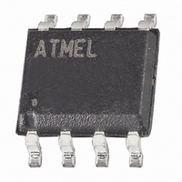
ATTINY13A-SU Atmel, ATTINY13A-SU Datasheet - Page 67

ATTINY13A-SU
Manufacturer Part Number
ATTINY13A-SU
Description
IC MCU AVR 1K FLASH 20MHZ 8SOIC
Manufacturer
Atmel
Series
AVR® ATtinyr
Specifications of ATTINY13A-SU
Core Processor
AVR
Core Size
8-Bit
Speed
20MHz
Peripherals
Brown-out Detect/Reset, POR, PWM, WDT
Number Of I /o
6
Program Memory Size
1KB (512 x 16)
Program Memory Type
FLASH
Eeprom Size
64 x 8
Ram Size
64 x 8
Voltage - Supply (vcc/vdd)
1.8 V ~ 5.5 V
Data Converters
A/D 4x10b
Oscillator Type
Internal
Operating Temperature
-40°C ~ 85°C
Package / Case
8-SOIC (5.3mm Width), 8-SOP, 8-SOEIAJ
Cpu Family
ATtiny
Device Core
AVR
Device Core Size
8b
Frequency (max)
20MHz
Interface Type
SPI
Total Internal Ram Size
64Byte
# I/os (max)
6
Number Of Timers - General Purpose
1
Operating Supply Voltage (typ)
2.5/3.3/5V
Operating Supply Voltage (max)
5.5V
Operating Supply Voltage (min)
1.8V
On-chip Adc
4-chx10-bit
Instruction Set Architecture
RISC
Operating Temp Range
-40C to 85C
Operating Temperature Classification
Industrial
Mounting
Surface Mount
Pin Count
8
Package Type
SOIC EIAJ
Processor Series
ATTINY1x
Core
AVR8
Data Bus Width
8 bit
Data Ram Size
64 B
Maximum Clock Frequency
20 MHz
Number Of Programmable I/os
6
Number Of Timers
1
Maximum Operating Temperature
+ 85 C
Mounting Style
SMD/SMT
3rd Party Development Tools
EWAVR, EWAVR-BL
Development Tools By Supplier
ATAVRDRAGON, ATSTK500, ATSTK600, ATAVRISP2, ATAVRONEKIT, ATAKSTK511
Minimum Operating Temperature
- 40 C
Package
8SOIC EIAJ
Family Name
ATtiny
Maximum Speed
20 MHz
Operating Supply Voltage
2.5|3.3|5 V
For Use With
ATSTK600-DIP40 - STK600 SOCKET/ADAPTER 40-PDIP770-1007 - ISP 4PORT ATMEL AVR MCU SPI/JTAG770-1004 - ISP 4PORT FOR ATMEL AVR MCU SPIATAVRDRAGON - KIT DRAGON 32KB FLASH MEM AVRATAVRISP2 - PROGRAMMER AVR IN SYSTEMATJTAGICE2 - AVR ON-CHIP D-BUG SYSTEM
Lead Free Status / RoHS Status
Lead free / RoHS Compliant
Connectivity
-
Lead Free Status / Rohs Status
Compliant
Available stocks
Company
Part Number
Manufacturer
Quantity
Price
Company:
Part Number:
ATTINY13A-SU
Manufacturer:
TI
Quantity:
21 550
Part Number:
ATTINY13A-SU
Manufacturer:
ATMEL/爱特梅尔
Quantity:
20 000
11.7.4
8126E–AVR–07/10
Phase Correct PWM Mode
in a constantly high or low output (depending on the polarity of the output set by the COM0A[1:0]
bits.)
A frequency (with 50% duty cycle) waveform output in fast PWM mode can be achieved by set-
ting OC0x to toggle its logical level on each Compare Match (COM0x[1:0] = 1). The waveform
generated will have a maximum frequency of f
feature is similar to the OC0A toggle in CTC mode, except the double buffer feature of the Out-
put Compare unit is enabled in the fast PWM mode.
The phase correct PWM mode (WGM0[2:0] = 1 or 5) provides a high resolution phase correct
PWM waveform generation option. The phase correct PWM mode is based on a dual-slope
operation. The counter counts repeatedly from BOTTOM to TOP and then from TOP to BOT-
TOM. TOP is defined as 0xFF when WGM0[2:0] = 1, and OCR0A when WGM0[2:0] = 5. In non-
inverting Compare Output mode, the Output Compare (OC0x) is cleared on the Compare Match
between TCNT0 and OCR0x while upcounting, and set on the Compare Match while down-
counting. In inverting Output Compare mode, the operation is inverted. The dual-slope operation
has lower maximum operation frequency than single slope operation. However, due to the sym-
metric feature of the dual-slope PWM modes, these modes are preferred for motor control
applications.
In phase correct PWM mode the counter is incremented until the counter value matches TOP.
When the counter reaches TOP, it changes the count direction. The TCNT0 value will be equal
to TOP for one timer clock cycle. The timing diagram for the phase correct PWM mode is shown
on
illustrating the dual-slope operation. The diagram includes non-inverted and inverted PWM out-
puts. The small horizontal line marks on the TCNT0 slopes represent Compare Matches
between OCR0x and TCNT0.
Figure 11-7. Phase Correct PWM Mode, Timing Diagram
TCNTn
OCn
OCn
Period
Figure 11-7 on page
67. The TCNT0 value is in the timing diagram shown as a histogram for
1
2
OC0
= f
clk_I/O
/2 when OCR0A is set to zero. This
3
OCnx Interrupt Flag Set
OCRnx Update
TOVn Interrupt Flag Set
(COMnx[1:0] = 2)
(COMnx[1:0] = 3)
67


