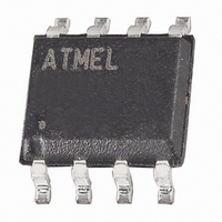
ATTINY13A-SU Atmel, ATTINY13A-SU Datasheet - Page 100

ATTINY13A-SU
Manufacturer Part Number
ATTINY13A-SU
Description
IC MCU AVR 1K FLASH 20MHZ 8SOIC
Manufacturer
Atmel
Series
AVR® ATtinyr
Specifications of ATTINY13A-SU
Core Processor
AVR
Core Size
8-Bit
Speed
20MHz
Peripherals
Brown-out Detect/Reset, POR, PWM, WDT
Number Of I /o
6
Program Memory Size
1KB (512 x 16)
Program Memory Type
FLASH
Eeprom Size
64 x 8
Ram Size
64 x 8
Voltage - Supply (vcc/vdd)
1.8 V ~ 5.5 V
Data Converters
A/D 4x10b
Oscillator Type
Internal
Operating Temperature
-40°C ~ 85°C
Package / Case
8-SOIC (5.3mm Width), 8-SOP, 8-SOEIAJ
Cpu Family
ATtiny
Device Core
AVR
Device Core Size
8b
Frequency (max)
20MHz
Interface Type
SPI
Total Internal Ram Size
64Byte
# I/os (max)
6
Number Of Timers - General Purpose
1
Operating Supply Voltage (typ)
2.5/3.3/5V
Operating Supply Voltage (max)
5.5V
Operating Supply Voltage (min)
1.8V
On-chip Adc
4-chx10-bit
Instruction Set Architecture
RISC
Operating Temp Range
-40C to 85C
Operating Temperature Classification
Industrial
Mounting
Surface Mount
Pin Count
8
Package Type
SOIC EIAJ
Processor Series
ATTINY1x
Core
AVR8
Data Bus Width
8 bit
Data Ram Size
64 B
Maximum Clock Frequency
20 MHz
Number Of Programmable I/os
6
Number Of Timers
1
Maximum Operating Temperature
+ 85 C
Mounting Style
SMD/SMT
3rd Party Development Tools
EWAVR, EWAVR-BL
Development Tools By Supplier
ATAVRDRAGON, ATSTK500, ATSTK600, ATAVRISP2, ATAVRONEKIT, ATAKSTK511
Minimum Operating Temperature
- 40 C
Package
8SOIC EIAJ
Family Name
ATtiny
Maximum Speed
20 MHz
Operating Supply Voltage
2.5|3.3|5 V
For Use With
ATSTK600-DIP40 - STK600 SOCKET/ADAPTER 40-PDIP770-1007 - ISP 4PORT ATMEL AVR MCU SPI/JTAG770-1004 - ISP 4PORT FOR ATMEL AVR MCU SPIATAVRDRAGON - KIT DRAGON 32KB FLASH MEM AVRATAVRISP2 - PROGRAMMER AVR IN SYSTEMATJTAGICE2 - AVR ON-CHIP D-BUG SYSTEM
Lead Free Status / RoHS Status
Lead free / RoHS Compliant
Connectivity
-
Lead Free Status / Rohs Status
Compliant
Available stocks
Company
Part Number
Manufacturer
Quantity
Price
Company:
Part Number:
ATTINY13A-SU
Manufacturer:
TI
Quantity:
21 550
Part Number:
ATTINY13A-SU
Manufacturer:
ATMEL/爱特梅尔
Quantity:
20 000
16.5
16.6
16.6.1
16.6.2
100
EEPROM Write Prevents Writing to SPMCSR
Reading Fuse and Lock Bits from Firmware
ATtiny13A
Reading Lock Bits from Firmware
Reading Fuse Bits from Firmware
The LPM instruction uses the Z-pointer to store the address. Since this instruction addresses the
Flash byte-by-byte, also the LSB (bit Z0) of the Z-pointer is used.
Note that an EEPROM write operation will block all software programming to Flash. Reading the
fuses and lock bits from software will also be prevented during the EEPROM write operation. It is
recommended that the user checks the status bit (EEPE) in the EECR Register and verifies that
the bit is cleared before writing to the SPMCSR Register.
It is possible to read fuse and lock bits from software.
Issuing an LPM instruction within three CPU cycles after RFLB and SELFPRGEN bits have
been set in SPMCSR will return lock bit values in the destination register. The RFLB and SELF-
PRGEN bits automatically clear upon completion of reading the lock bits, or if no LPM instruction
is executed within three CPU cycles, or if no SPM instruction is executed within four CPU cycles.
When RFLB and SELFPRGEN are cleared, LPM functions normally.
To read the lock bits, follow the below procedure.
If successful, the contents of the destination register are as follows.
See section
bits.
The algorithm for reading fuse bytes is similar to the one described above for reading lock bits,
only the addresses are different.
To read the Fuse Low Byte (FLB), follow the below procedure:
If successful, the contents of the destination register are as follows.
Bit
Rd
Bit
Rd
1. Load the Z-pointer with 0x0001.
2. Set RFLB and SELFPRGEN bits in SPMCSR.
3. Issuing an LPM instruction within three clock cycles will return lock bits in the destina-
1. Load the Z-pointer with 0x0000.
2. Set RFLB and SELFPRGEN bits in SPMCSR.
3. Issuing an LPM instruction within three clock cycles will FLB in the destination register.
tion register.
“Program And Data Memory Lock Bits” on page 103
FLB7
7
–
7
FLB6
6
–
6
FLB5
5
5
–
FLB4
4
–
4
FLB3
3
–
3
FLB2
2
–
2
for more information on lock
FLB1
LB2
1
1
FLB0
LB1
0
0
8126E–AVR–07/10


