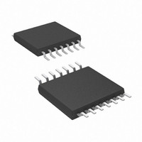
AT89LP214-20XU Atmel, AT89LP214-20XU Datasheet - Page 7

AT89LP214-20XU
Manufacturer Part Number
AT89LP214-20XU
Description
MCU 8051 2K FLASH 20MHZ 14-TSSOP
Manufacturer
Atmel
Series
89LPr
Datasheet
1.AT89LP213-20PU.pdf
(98 pages)
Specifications of AT89LP214-20XU
Core Processor
8051
Core Size
8-Bit
Speed
20MHz
Connectivity
SPI, UART/USART
Peripherals
Brown-out Detect/Reset, POR, PWM, WDT
Number Of I /o
12
Program Memory Size
2KB (2K x 8)
Program Memory Type
FLASH
Ram Size
128 x 8
Voltage - Supply (vcc/vdd)
2.4 V ~ 5.5 V
Oscillator Type
Internal
Operating Temperature
-40°C ~ 85°C
Package / Case
14-TSSOP
Package
14TSSOP
Device Core
8051
Family Name
AT89
Maximum Speed
20 MHz
Operating Supply Voltage
2.5|3.3|5 V
Data Bus Width
8 Bit
Number Of Programmable I/os
12
Interface Type
SPI/UART
Number Of Timers
2
Core
8051
Processor Series
AT89x
Maximum Clock Frequency
20 MHz
Data Ram Size
128 B
Mounting Style
SMD/SMT
Height
1.05 mm
Length
5.1 mm
Maximum Operating Temperature
+ 85 C
Minimum Operating Temperature
- 40 C
Supply Voltage (max)
5.5 V
Supply Voltage (min)
2.4 V
Width
4.5 mm
Lead Free Status / RoHS Status
Lead free / RoHS Compliant
Eeprom Size
-
Data Converters
-
Lead Free Status / Rohs Status
Details
5.6
5.7
5.8
6. Memory Organization
6.1
3538E–MICRO–11/10
Watchdog Timer
I/O Ports
Reset
Program Memory
The Watchdog Timer in AT89LP213/214 counts at a rate of once per clock cycle. This compares
to once every 12 clocks in the standard 8051. A common prescaler is available to divide the time
base for all timers and reduce the counting rate.
The I/O ports of the AT89LP213/214 may be configured in four different modes. By default all
the I/O ports revert to input-only (tristated) mode at power-up or reset. In the standard 8051, all
ports are weakly pulled high during power-up or reset. To enable 8051-like ports, the ports must
be put into quasi-bidirectional mode by clearing the P1M0 and P3M0 SFRs. The user can also
configure the ports to start in quasi-bidirectional mode by disabling the Tristate-Port User Fuse.
When this fuse is disabled, P1M0 and P3M0 will reset to 00h instead of FFh and the ports will be
weakly pulled high.
The RST pin of the AT89LP213/214 is active-low as compared with the active high reset in the
standard 8051. In addition, the RST pin is sampled every clock cycle and must be held low for a
minimum of two clock cycles, instead of 24 clock cycles, to be recognized as a valid reset.
The AT89LP213/214 uses a Harvard Architecture with separate address spaces for program
and data memory. The program memory has a regular linear address space with support for up
to 64K bytes of directly addressable application code. The data memory has 128 bytes of inter-
nal RAM and 128 bytes of Special Function Register I/O space. The AT89LP213/214 does not
support external data memory or external program memory.
The AT89LP213/214 contains 2K bytes of on-chip In-System Programmable Flash memory for
program storage. The Flash memory has an endurance of at least 10,000 write/erase cycles and
a minimum data retention time of 10 years. The reset and interrupt vectors are located within the
first 59 bytes of program memory (refer to
cated within the entire 2K program memory address space for access by the MOVC instruction.
The AT89LP213/214 does not support external program memory.
Figure 6-1.
Program Memory Map
0040
0000
0000
007F
001F
07FF
Atmel Signature Array
User Signature Array
Table 12-1 on page
Program Memory
20). Constant tables can be allo-
AT89LP213/214
7


