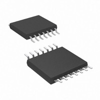
AT89LP214-20XU Atmel, AT89LP214-20XU Datasheet - Page 16

AT89LP214-20XU
Manufacturer Part Number
AT89LP214-20XU
Description
MCU 8051 2K FLASH 20MHZ 14-TSSOP
Manufacturer
Atmel
Series
89LPr
Datasheet
1.AT89LP213-20PU.pdf
(98 pages)
Specifications of AT89LP214-20XU
Core Processor
8051
Core Size
8-Bit
Speed
20MHz
Connectivity
SPI, UART/USART
Peripherals
Brown-out Detect/Reset, POR, PWM, WDT
Number Of I /o
12
Program Memory Size
2KB (2K x 8)
Program Memory Type
FLASH
Ram Size
128 x 8
Voltage - Supply (vcc/vdd)
2.4 V ~ 5.5 V
Oscillator Type
Internal
Operating Temperature
-40°C ~ 85°C
Package / Case
14-TSSOP
Package
14TSSOP
Device Core
8051
Family Name
AT89
Maximum Speed
20 MHz
Operating Supply Voltage
2.5|3.3|5 V
Data Bus Width
8 Bit
Number Of Programmable I/os
12
Interface Type
SPI/UART
Number Of Timers
2
Core
8051
Processor Series
AT89x
Maximum Clock Frequency
20 MHz
Data Ram Size
128 B
Mounting Style
SMD/SMT
Height
1.05 mm
Length
5.1 mm
Maximum Operating Temperature
+ 85 C
Minimum Operating Temperature
- 40 C
Supply Voltage (max)
5.5 V
Supply Voltage (min)
2.4 V
Width
4.5 mm
Lead Free Status / RoHS Status
Lead free / RoHS Compliant
Eeprom Size
-
Data Converters
-
Lead Free Status / Rohs Status
Details
10.2
10.3
16
Brown-out Reset
External Reset
AT89LP213/214
Table 10-1.
The AT89LP213/214 has an on-chip Brown-out Detection (BOD) circuit for monitoring the V
level during operation by comparing it to a fixed trigger level. The trigger level for the BOD is
nominally 2.2V. The purpose of the BOD is to ensure that if V
speed, the system will gracefully enter reset without the possibility of errors induced by incorrect
execution. A BOD sequence is shown in
trigger level V
trigger level, the start-up timer releases the internal reset after the specified time-out period has
expired
(See “User Configuration Fuses” on page
Figure 10-3. Brown-out Detector Reset
The P1.3/RST pin can function as either an active-LOW reset input or as a digital general pur-
pose I/O, P1.3. The Reset Pin Enable Fuse, when set to “1”, enables the external reset input
function on P1.3.
used as an input or output pin. When configured as a reset input, the pin must be held low for at
least two clock cycles to trigger the internal reset.
Note:
INTERNAL
TIME-OUT
SUT Fuse 1
RESET
V
0
0
1
1
(Table
During a power-up sequence, the fuse selection is always overridden and therefore the pin will
always function as a reset input. An external circuit connected to this pin should not hold this
pin LOW during a power-on sequence as this will keep the device in reset until the pin tran-
sitions high. After the power-up delay, this input will function either as an external reset input or
as a digital input as defined by the fuse bit. Only a power-up reset will temporarily override the
selection defined by the reset fuse bit. Other sources of reset will not override the reset fuse bit.
P1.3/RST also serves as the In-System Programming (ISP) enable. ISP is enabled when the
external reset pin is held low. When the reset pin is disabled by the fuse, ISP may only be entered
by pulling P1.3 low during power-up.
CC
BOD
V POR
Start-up Timer Settings
10-1). The Brown-out Detector must be enabled by setting the BOD Enable Fuse.
, the internal reset is immediately activated. When V
(See “User Configuration Fuses” on page
SUT Fuse 0
0
1
0
1
Clock Source
Internal RC/External Clock
Crystal Oscillator
Internal RC/External Clock
Crystal Oscillator
Internal RC/External Clock
Crystal Oscillator
Internal RC/External Clock
Crystal Oscillator
Figure
72).
V BOD
t SUT
10-3. When V
CC
72). When cleared, P1.3 may be
CC
decreases to a value below the
fails or dips while executing at
CC
increases above the
t
16 µs
1024 µs
512 µs
2048 µs
1024 µs
4096 µs
4096 µs
16384 µs
SUT
(± 5%)
3538E–MICRO–11/10
CC


