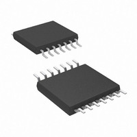
AT89LP214-20XU Atmel, AT89LP214-20XU Datasheet - Page 26

AT89LP214-20XU
Manufacturer Part Number
AT89LP214-20XU
Description
MCU 8051 2K FLASH 20MHZ 14-TSSOP
Manufacturer
Atmel
Series
89LPr
Datasheet
1.AT89LP213-20PU.pdf
(98 pages)
Specifications of AT89LP214-20XU
Core Processor
8051
Core Size
8-Bit
Speed
20MHz
Connectivity
SPI, UART/USART
Peripherals
Brown-out Detect/Reset, POR, PWM, WDT
Number Of I /o
12
Program Memory Size
2KB (2K x 8)
Program Memory Type
FLASH
Ram Size
128 x 8
Voltage - Supply (vcc/vdd)
2.4 V ~ 5.5 V
Oscillator Type
Internal
Operating Temperature
-40°C ~ 85°C
Package / Case
14-TSSOP
Package
14TSSOP
Device Core
8051
Family Name
AT89
Maximum Speed
20 MHz
Operating Supply Voltage
2.5|3.3|5 V
Data Bus Width
8 Bit
Number Of Programmable I/os
12
Interface Type
SPI/UART
Number Of Timers
2
Core
8051
Processor Series
AT89x
Maximum Clock Frequency
20 MHz
Data Ram Size
128 B
Mounting Style
SMD/SMT
Height
1.05 mm
Length
5.1 mm
Maximum Operating Temperature
+ 85 C
Minimum Operating Temperature
- 40 C
Supply Voltage (max)
5.5 V
Supply Voltage (min)
2.4 V
Width
4.5 mm
Lead Free Status / RoHS Status
Lead free / RoHS Compliant
Eeprom Size
-
Data Converters
-
Lead Free Status / Rohs Status
Details
13.1.4
13.2
26
Port 1 Analog Functions
AT89LP213/214
Push-pull Output
Figure 13-4. Open-drain Output
The push-pull output configuration has the same pull-down structure as both the open-drain and
the quasi-bidirectional output modes, but provides a continuous strong pull-up when the port
latch contains a logic “1”. The push-pull mode may be used when more source current is needed
from a port output. Note that due to the 5V tolerant architecture, the push-pull output will have
reduced output high levels at DC operation and hot temperature. Under AC operation an inter-
grated boost circuit provides more source current. The push-pull port configuration is shown in
Figure
Figure
Figure 13-5. Push-pull Output
The AT89LP213/214 incorporates an analog comparator. In order to give the best analog perfor-
mance and minimize power consumption, pins that are being used for analog functions must
have both their digital outputs and digital inputs disabled. Digital outputs are disabled by putting
the port pins into the input-only mode as described in
inputs on P1.0 and P1.1 are disabled whenever the Analog Comparator is enabled by setting the
CEN bit in ACSR. CEN forces the PWD input on P1.0 and P1.1 low, thereby disabling the
Schmitt trigger circuitry. P1.0 and P1.1 will always default to input-only mode after reset regard-
less of the state of the Tristate-Port Fuse.
13-5. The input circuitry of P1.3, P3.2 and P3.3 is not disabled during Power-down (see
13-3).
Register
From Port
From Port
Register
Input
Data
PWD
Input
Data
V
PWD
CC
“Port Configuration” on page
Port
Pin
3538E–MICRO–11/10
Port
Pin
24. Digital


