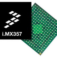
MCIMX357CJQ5C Freescale Semiconductor, MCIMX357CJQ5C Datasheet - Page 14

MCIMX357CJQ5C
Manufacturer Part Number
MCIMX357CJQ5C
Description
MPU MX35 ARM11 400-MAPBGA
Manufacturer
Freescale Semiconductor
Series
i.MX35r
Specifications of MCIMX357CJQ5C
Core Processor
ARM11
Core Size
32-Bit
Speed
532MHz
Connectivity
1-Wire, CAN, EBI/EMI, Ethernet, I²C, MMC, SPI, SSI, UART/USART, USB OTG
Peripherals
DMA, I²S, LCD, POR, PWM, WDT
Number Of I /o
96
Program Memory Type
ROMless
Ram Size
128K x 8
Voltage - Supply (vcc/vdd)
1.33 V ~ 1.47 V
Oscillator Type
External
Operating Temperature
-40°C ~ 85°C
Package / Case
400-MAPBGA
Processor Series
i.MX357
Core
ARM1136JF-S
Data Bus Width
32 bit
Data Ram Size
128 KB
Interface Type
I2C, JTAG, UART
Maximum Clock Frequency
532 MHz
Number Of Timers
3
Operating Supply Voltage
1.33 V to 1.47 V
Maximum Operating Temperature
+ 85 C
Mounting Style
SMD/SMT
Minimum Operating Temperature
- 40 C
Lead Free Status / RoHS Status
Lead free / RoHS Compliant
Eeprom Size
-
Program Memory Size
-
Data Converters
-
Lead Free Status / Rohs Status
Details
Available stocks
Company
Part Number
Manufacturer
Quantity
Price
Company:
Part Number:
MCIMX357CJQ5C
Manufacturer:
Freescale Semiconductor
Quantity:
10 000
Company:
Part Number:
MCIMX357CJQ5CR2
Manufacturer:
Freescale Semiconductor
Quantity:
10 000
1
2
3
4.1.2
Table 9
14
I2Sx2,ESAI, I2C2, UART2, UART1, FEC
MLB
USB OTG PHY
USB OTG PHY
USB OTG PHY
USB HOST PHY
OSC24M
OSC_AUDIO
MPLL
PPLL
Fusebox program supply voltage
Operating Ambient Temperature Range
Operating Ambient Temperature Range
EMI I/O interface power supply should be set up according to external memory. For example, if using SDRAM then
NVCC_EMI1,2,3 should all be set at 3.3 V (typ.). If using MDDR or DDR2, NVC_EMI1,2,3 must be set at 1.8 V (typ.).
MLB Interface I/O pins can be programmed to function as GPIO for the consumer and industrial parts by setting NVCC_MLB
to 1.8 or 3.3 V. NVCC_MLB can be left floating.
The Fusebox read supply is connected to supply of the full speed USB PHY. FUSE_VDD is only used for programming. It is
recommended that FUSE_VDD be connected to ground when not being used for programming. FUSE_VDD should be
supplied by following the power up sequence given in
ID
1
provides information on interface frequency limits.
JTAG TCK Frequency
Interface Frequency Limits
i.MX35 Applications Processors for Industrial and Consumer Products, Rev. 9
Parameter
Parameter
Table 8. i.MX35 Operating Ranges (continued)
Table 9. Interface Frequency
Section 4.3.1, “Powering Up.”
Symbol
f
NVCC_MISC
NVCC_MLB
OSC24M_VDD
OSC_AUDIO_VDD
MVDD
PVDD
FUSE_VDD
T
T
PHY1_VDDA
USBPHY1_VDDA_BIAS
USBPHY1_UPLLVDD
PHY2_VDD
JTAG
A
A
Symbol
3
2
Min.
DC
Min.
1.75
1.75
3.17
3.17
3.17
–20
–40
3.0
3.0
3.0
1.4
1.4
3.0
Typ.
5
Typical
Freescale Semiconductor
3.3
3.3
3.3
3.3
3.3
3.3
3.6
—
—
—
—
—
—
Max.
10
Max.
3.43
3.43
3.43
1.65
1.65
3.6
3.6
3.6
3.6
3.6
3.6
70
85
Units
MHz
Units
o
o
V
V
V
V
V
V
V
V
V
V
V
C
C


