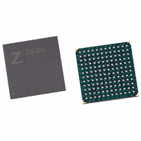
EZ80F91NA050EC Zilog, EZ80F91NA050EC Datasheet - Page 90
EZ80F91NA050EC
Manufacturer Part Number
EZ80F91NA050EC
Description
IC ACCLAIM MCU 256KB 144-BGA
Manufacturer
Zilog
Series
eZ80® Acclaim!®r
Specifications of EZ80F91NA050EC
Core Processor
Z8
Core Size
8-Bit
Speed
50MHz
Connectivity
Ethernet, I²C, IrDA, SPI, UART/USART
Peripherals
Brown-out Detect/Reset, POR, PWM, WDT
Number Of I /o
32
Program Memory Size
256KB (256K x 8)
Program Memory Type
FLASH
Ram Size
16K x 8
Voltage - Supply (vcc/vdd)
3 V ~ 3.6 V
Oscillator Type
Internal
Operating Temperature
-40°C ~ 105°C
Package / Case
144-LBGA
Data Bus Width
8 bit
Maximum Clock Frequency
50 MHz
Number Of Programmable I/os
32
Number Of Timers
16 bit
Operating Supply Voltage
3 V to 3.6 V
Maximum Operating Temperature
+ 105 C
Mounting Style
SMD/SMT
Minimum Operating Temperature
- 40 C
For Use With
269-4712 - KIT DEV ENCORE 32 SERIES269-4671 - BOARD ZDOTS SBC Z80ACCLAIM PLUS269-4561 - KIT DEV FOR EZ80F91 W/C-COMPILER269-4560 - KIT DEV FOR EZ80F91 W/C-COMPILER
Lead Free Status / RoHS Status
Contains lead / RoHS non-compliant
Eeprom Size
-
Data Converters
-
Lead Free Status / Rohs Status
No
Other names
269-3250
Available stocks
Company
Part Number
Manufacturer
Quantity
Price


Table 25. Motorola Bus Mode Read States
PS019215-0910
STATE S0
STATE S1
STATE S2
STATE S3
STATE S4
STATE S5
The Read cycle starts in state S0. The CPU drives R/W High to identify a Read cycle.
Entering state S1, the CPU drives a valid address on the address bus, ADDR[23:0].
During state S3, no bus signals are altered.
During state S4, the CPU waits for a cycle termination signal DTACK (WAIT), a peripheral
During state S5, no bus signals are altered.
On the rising edge of state S2, the CPU asserts AS and DS.
signal. If the termination signal is not asserted at least one full CPU clock period prior to the
rising clock edge at the end of S4, the CPU inserts WAIT (T
asserted. Each wait state is a full bus mode cycle.
During Write operations, the Motorola bus mode employs eight states—S0, S1, S2, S3,
S4, S5, S6, and S7 as listed in
eZ80 Bus Mode
Signals (Pins)
ADDR[23:0]
DATA[7:0]
INSTRD
MREQ
IORQ
WAIT
WR
RD
Figure 17. Motorola Bus Mode Signal and Pin Mapping
Table
Bus Mode
Controller
25.
WAIT
Motorola Bus
Signal Equvalents
AS
DS
R/W
DTACK
MREQ
IORQ
ADDR[23:0]
DATA[7:0]
) states until DTACK is
Chip Selects and Wait States
Product Specification
eZ80F91 MCU
81
Related parts for EZ80F91NA050EC
Image
Part Number
Description
Manufacturer
Datasheet
Request
R

Part Number:
Description:
Communication Controllers, ZILOG INTELLIGENT PERIPHERAL CONTROLLER (ZIP)
Manufacturer:
Zilog, Inc.
Datasheet:

Part Number:
Description:
KIT DEV FOR Z8 ENCORE 16K TO 64K
Manufacturer:
Zilog
Datasheet:

Part Number:
Description:
KIT DEV Z8 ENCORE XP 28-PIN
Manufacturer:
Zilog
Datasheet:

Part Number:
Description:
DEV KIT FOR Z8 ENCORE 8K/4K
Manufacturer:
Zilog
Datasheet:

Part Number:
Description:
KIT DEV Z8 ENCORE XP 28-PIN
Manufacturer:
Zilog
Datasheet:

Part Number:
Description:
DEV KIT FOR Z8 ENCORE 4K TO 8K
Manufacturer:
Zilog
Datasheet:
Part Number:
Description:
CMOS Z8 microcontroller. ROM 16 Kbytes, RAM 256 bytes, speed 16 MHz, 32 lines I/O, 3.0V to 5.5V
Manufacturer:
Zilog, Inc.
Datasheet:
Part Number:
Description:
Low-cost microcontroller. 512 bytes ROM, 61 bytes RAM, 8 MHz
Manufacturer:
Zilog, Inc.
Datasheet:
Part Number:
Description:
Z8 4K OTP Microcontroller
Manufacturer:
Zilog, Inc.
Datasheet:
Part Number:
Description:
CMOS SUPER8 ROMLESS MCU
Manufacturer:
Zilog, Inc.
Datasheet:
Part Number:
Description:
SL1866 CMOSZ8 OTP Microcontroller
Manufacturer:
Zilog, Inc.
Datasheet:
Part Number:
Description:
SL1866 CMOSZ8 OTP Microcontroller
Manufacturer:
Zilog, Inc.
Datasheet:
Part Number:
Description:
OTP (KB) = 1, RAM = 125, Speed = 12, I/O = 14, 8-bit Timers = 2, Comm Interfaces Other Features = Por, LV Protect, Voltage = 4.5-5.5V
Manufacturer:
Zilog, Inc.
Datasheet:
Part Number:
Description:
Manufacturer:
Zilog, Inc.
Datasheet: