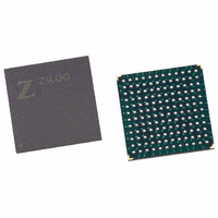
EZ80F91NA050EC Zilog, EZ80F91NA050EC Datasheet - Page 273

EZ80F91NA050EC
Manufacturer Part Number
EZ80F91NA050EC
Description
IC ACCLAIM MCU 256KB 144-BGA
Manufacturer
Zilog
Series
eZ80® Acclaim!®r
Specifications of EZ80F91NA050EC
Core Processor
Z8
Core Size
8-Bit
Speed
50MHz
Connectivity
Ethernet, I²C, IrDA, SPI, UART/USART
Peripherals
Brown-out Detect/Reset, POR, PWM, WDT
Number Of I /o
32
Program Memory Size
256KB (256K x 8)
Program Memory Type
FLASH
Ram Size
16K x 8
Voltage - Supply (vcc/vdd)
3 V ~ 3.6 V
Oscillator Type
Internal
Operating Temperature
-40°C ~ 105°C
Package / Case
144-LBGA
Data Bus Width
8 bit
Maximum Clock Frequency
50 MHz
Number Of Programmable I/os
32
Number Of Timers
16 bit
Operating Supply Voltage
3 V to 3.6 V
Maximum Operating Temperature
+ 105 C
Mounting Style
SMD/SMT
Minimum Operating Temperature
- 40 C
For Use With
269-4712 - KIT DEV ENCORE 32 SERIES269-4671 - BOARD ZDOTS SBC Z80ACCLAIM PLUS269-4561 - KIT DEV FOR EZ80F91 W/C-COMPILER269-4560 - KIT DEV FOR EZ80F91 W/C-COMPILER
Lead Free Status / RoHS Status
Contains lead / RoHS non-compliant
Eeprom Size
-
Data Converters
-
Lead Free Status / Rohs Status
No
Other names
269-3250
Available stocks
Company
Part Number
Manufacturer
Quantity
Price
- Current page: 273 of 384
- Download datasheet (3Mb)
Table 151. Pin to Boundary Scan Cell Mapping (Continued)
PS019215-0910
Pin
MII_Tx_ER
MII_Tx_CLK
MII_Tx_EN
MII_TxD0
MII_TxD1
Notes
1. The address bits 0–7, 8–15, and 16–23 each share a single output enable. In this table, the output enables are
2. Direction on the data bus is controlled by a single output enable. It is associated in this table with D[0].
3. MREQ,
associated with the LSb that they control.
IORQ
Usage
Boundary scan functionality is utilized by issuing the appropriate Test Access Port (TAP)
instruction and shifting data accordingly. Both of these steps are accomplished using the
JTAG interface. To activate the TAP (see
be driven Low at least two CPU system clock cycles prior to the deassertion of the RESET
pin. Otherwise the OCI-JTAG features are disabled.
As per the IEEE 1149.1 specification, the boundary scan cells capture system I/O on the
rising edge of TCK during the CAPTURE_DR state. This captured data is shifted on the
rising edge of TCK while in the SHIFT_DR state. Pins and logic receive shifted data only
when enabled, and only on the falling edge of TCK during the UPDATE_DR state, after
shifting is completed.
For more information about eZ80F91 boundary scan support, refer to Using BSDL Files
with eZ80
Boundary Scan Instructions
The eZ80F91 device’s boundary scan architecture supports the following instructions:
•
•
•
•
•
, INSTRDN, RD, and WR share an output enable; it is associated in this table with WR.
BYPASS (required)
SAMPLE (required)
EXTEST (required)
PRELOAD (required)
IDCODE (optional)
Direction
Output
Output
Output
Output
Input
®
and eZ80Acclaim!
Scan Cell No
102
103
104
105
106
®
Devices (AN0114).
Pin
PD1
PD0
PD0
PD0
OCI Activation
on page 258), the TCK pin must
Direction
Output
Product Specification
Input
OEN
OEN
On-Chip Instrumentation
eZ80F91 MCU
Scan Cell No
209
210
212
211
264
Related parts for EZ80F91NA050EC
Image
Part Number
Description
Manufacturer
Datasheet
Request
R

Part Number:
Description:
Communication Controllers, ZILOG INTELLIGENT PERIPHERAL CONTROLLER (ZIP)
Manufacturer:
Zilog, Inc.
Datasheet:

Part Number:
Description:
KIT DEV FOR Z8 ENCORE 16K TO 64K
Manufacturer:
Zilog
Datasheet:

Part Number:
Description:
KIT DEV Z8 ENCORE XP 28-PIN
Manufacturer:
Zilog
Datasheet:

Part Number:
Description:
DEV KIT FOR Z8 ENCORE 8K/4K
Manufacturer:
Zilog
Datasheet:

Part Number:
Description:
KIT DEV Z8 ENCORE XP 28-PIN
Manufacturer:
Zilog
Datasheet:

Part Number:
Description:
DEV KIT FOR Z8 ENCORE 4K TO 8K
Manufacturer:
Zilog
Datasheet:

Part Number:
Description:
CMOS Z8 microcontroller. ROM 16 Kbytes, RAM 256 bytes, speed 16 MHz, 32 lines I/O, 3.0V to 5.5V
Manufacturer:
Zilog, Inc.
Datasheet:

Part Number:
Description:
Low-cost microcontroller. 512 bytes ROM, 61 bytes RAM, 8 MHz
Manufacturer:
Zilog, Inc.
Datasheet:

Part Number:
Description:
Z8 4K OTP Microcontroller
Manufacturer:
Zilog, Inc.
Datasheet:

Part Number:
Description:
CMOS SUPER8 ROMLESS MCU
Manufacturer:
Zilog, Inc.
Datasheet:

Part Number:
Description:
SL1866 CMOSZ8 OTP Microcontroller
Manufacturer:
Zilog, Inc.
Datasheet:

Part Number:
Description:
SL1866 CMOSZ8 OTP Microcontroller
Manufacturer:
Zilog, Inc.
Datasheet:

Part Number:
Description:
OTP (KB) = 1, RAM = 125, Speed = 12, I/O = 14, 8-bit Timers = 2, Comm Interfaces Other Features = Por, LV Protect, Voltage = 4.5-5.5V
Manufacturer:
Zilog, Inc.
Datasheet:

Part Number:
Description:
Manufacturer:
Zilog, Inc.
Datasheet:


