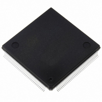
ST10F272Z2Q3 STMicroelectronics, ST10F272Z2Q3 Datasheet - Page 45

ST10F272Z2Q3
Manufacturer Part Number
ST10F272Z2Q3
Description
MCU 16BIT 256KB FLASH 144-PQFP
Manufacturer
STMicroelectronics
Series
ST10r
Datasheet
1.ST10F272Z2Q3.pdf
(189 pages)
Specifications of ST10F272Z2Q3
Core Processor
ST10
Core Size
16-Bit
Speed
64MHz
Connectivity
ASC, CAN, EBI/EMI, I²C, SSC, UART/USART
Peripherals
POR, PWM, WDT
Number Of I /o
111
Program Memory Size
256KB (256K x 8)
Program Memory Type
FLASH
Ram Size
20K x 8
Voltage - Supply (vcc/vdd)
4.5 V ~ 5.5 V
Data Converters
A/D 24x10b
Oscillator Type
Internal
Operating Temperature
-40°C ~ 125°C
Package / Case
144-QFP
Lead Free Status / RoHS Status
Lead free / RoHS Compliant
Eeprom Size
-
Other names
497-5579
Available stocks
Company
Part Number
Manufacturer
Quantity
Price
Company:
Part Number:
ST10F272Z2Q3
Manufacturer:
E-CMOS
Quantity:
10 000
Company:
Part Number:
ST10F272Z2Q3
Manufacturer:
STMicroelectronics
Quantity:
10 000
- Current page: 45 of 189
- Download datasheet (4Mb)
ST10F272Z2
5.7
Write operation summary
In general, each write operation is started through a sequence of 3 steps:
1.
2.
3.
Once selected, but not yet started, one operation can be canceled by resetting the operation
selection bit.
A summary of the available Flash Module Write Operations are shown in the following
Table
Table 25.
Word Program (32-bit)
Double Word Program (64-bit)
Sector Erase
Set Protection
Program/Erase Suspend
The first instruction is used to select the desired operation by setting its corresponding
selection bit in the Flash Control Register 0.
The second step is the definition of the Address and Data for programming or the
Sectors or Banks to erase.
The last instruction is used to start the write operation, by setting the start bit WMS in
the FCR0.
25.
Operation
Flash write operations
Select bit
DWPG
SUSP
WPG
SER
SPR
Address and data
FDR0L/FDR0H
FDR0L/FDR0H
FDR1L/FDR1H
FCR1L/FCR1H
FDR0L/FDR0H
FARL/FARH
FARL/FARH
None
Internal Flash memory
Start bit
WMS
WMS
WMS
WMS
None
45/189
Related parts for ST10F272Z2Q3
Image
Part Number
Description
Manufacturer
Datasheet
Request
R

Part Number:
Description:
STMicroelectronics [RIPPLE-CARRY BINARY COUNTER/DIVIDERS]
Manufacturer:
STMicroelectronics
Datasheet:

Part Number:
Description:
STMicroelectronics [LIQUID-CRYSTAL DISPLAY DRIVERS]
Manufacturer:
STMicroelectronics
Datasheet:

Part Number:
Description:
BOARD EVAL FOR MEMS SENSORS
Manufacturer:
STMicroelectronics
Datasheet:

Part Number:
Description:
NPN TRANSISTOR POWER MODULE
Manufacturer:
STMicroelectronics
Datasheet:

Part Number:
Description:
TURBOSWITCH ULTRA-FAST HIGH VOLTAGE DIODE
Manufacturer:
STMicroelectronics
Datasheet:

Part Number:
Description:
Manufacturer:
STMicroelectronics
Datasheet:

Part Number:
Description:
DIODE / SCR MODULE
Manufacturer:
STMicroelectronics
Datasheet:

Part Number:
Description:
DIODE / SCR MODULE
Manufacturer:
STMicroelectronics
Datasheet:

Part Number:
Description:
Search -----> STE16N100
Manufacturer:
STMicroelectronics
Datasheet:

Part Number:
Description:
Search ---> STE53NA50
Manufacturer:
STMicroelectronics
Datasheet:

Part Number:
Description:
NPN Transistor Power Module
Manufacturer:
STMicroelectronics
Datasheet:


