ST10F272Z2Q3 STMicroelectronics, ST10F272Z2Q3 Datasheet - Page 29
ST10F272Z2Q3
Manufacturer Part Number
ST10F272Z2Q3
Description
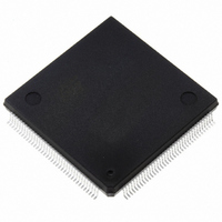
MCU 16BIT 256KB FLASH 144-PQFP
Manufacturer
STMicroelectronics
Series
ST10r
Datasheet
1.ST10F272Z2Q3.pdf
(189 pages)
Specifications of ST10F272Z2Q3
Core Processor
ST10
Core Size
16-Bit
Speed
64MHz
Connectivity
ASC, CAN, EBI/EMI, I²C, SSC, UART/USART
Peripherals
POR, PWM, WDT
Number Of I /o
111
Program Memory Size
256KB (256K x 8)
Program Memory Type
FLASH
Ram Size
20K x 8
Voltage - Supply (vcc/vdd)
4.5 V ~ 5.5 V
Data Converters
A/D 24x10b
Oscillator Type
Internal
Operating Temperature
-40°C ~ 125°C
Package / Case
144-QFP
Lead Free Status / RoHS Status
Lead free / RoHS Compliant
Eeprom Size
-
Other names
497-5579
Available stocks
Company
Part Number
Manufacturer
Quantity
Price
Company:

Part Number:
ST10F272Z2Q3
Manufacturer:
E-CMOS
Quantity:
10 000
Company:
Part Number:
ST10F272Z2Q3
Manufacturer:
STMicroelectronics
Quantity:
10 000


ST10F272Z2
5.3
Write operation
The Flash module have one single register interface mapped in the memory space of the
IBUS (0x08 0000 to 0x08 0015). All the operations are enabled through four 16-bit control
registers: Flash Control Register 1-0 High/Low (FCR1H/L-FCR0H/L). Eight other 16-bit
registers are used to store Flash Address and Data for Program operations (FARH/L and
FDR1H/L-FDR0H/L) and Write Operation Error flags (FERH/L). All registers are accessible
with 8 and 16-bit instructions (since operates in 16-bit mode when in read/ write).
Before accessing the IFlash module (and consequently also the Flash register to be used for
program/erasing operations), bit ROMEN in SYSCON register shall be set.
During a Flash write operation any attempt to read the flash itself, that is under modification,
will output invalid data (software trap 009Bh). This means that the Flash is not fetchable
when a programming operation is active: the write operation commands must be executed
from another memory (internal RAM or external memory), as in ST10F269 device. In fact,
due to IBUS characteristics, it is not possible to perform a write operation on IFLASH, when
fetching code from IFLASH.
Direct addressing is not allowed for write accesses to IFLASH Control Registers.
During a Write operation, when bit LOCK of FCR0 is set, it is forbidden to write into the
Flash Control Registers.
Power supply drop
If during a write operation the internal low voltage supply drops below a certain internal
voltage threshold, any write operation running is suddenly interrupted and the module is
reset to Read mode. At following Power-on, the interrupted Flash write operation must be
repeated.
Internal Flash memory
29/189
Related parts for ST10F272Z2Q3
Image
Part Number
Description
Manufacturer
Datasheet
Request
R

Part Number:
Description:
STMicroelectronics [RIPPLE-CARRY BINARY COUNTER/DIVIDERS]
Manufacturer:
STMicroelectronics
Datasheet:
Part Number:
Description:
STMicroelectronics [LIQUID-CRYSTAL DISPLAY DRIVERS]
Manufacturer:
STMicroelectronics
Datasheet:

Part Number:
Description:
BOARD EVAL FOR MEMS SENSORS
Manufacturer:
STMicroelectronics
Datasheet:
Part Number:
Description:
NPN TRANSISTOR POWER MODULE
Manufacturer:
STMicroelectronics
Datasheet:
Part Number:
Description:
TURBOSWITCH ULTRA-FAST HIGH VOLTAGE DIODE
Manufacturer:
STMicroelectronics
Datasheet:
Part Number:
Description:
Manufacturer:
STMicroelectronics
Datasheet:
Part Number:
Description:
DIODE / SCR MODULE
Manufacturer:
STMicroelectronics
Datasheet:
Part Number:
Description:
DIODE / SCR MODULE
Manufacturer:
STMicroelectronics
Datasheet:
Part Number:
Description:
Search -----> STE16N100
Manufacturer:
STMicroelectronics
Datasheet:
Part Number:
Description:
Search ---> STE53NA50
Manufacturer:
STMicroelectronics
Datasheet:
Part Number:
Description:
NPN Transistor Power Module
Manufacturer:
STMicroelectronics
Datasheet: