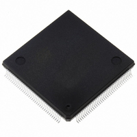
ST10F272Z2Q3 STMicroelectronics, ST10F272Z2Q3 Datasheet - Page 28

ST10F272Z2Q3
Manufacturer Part Number
ST10F272Z2Q3
Description
MCU 16BIT 256KB FLASH 144-PQFP
Manufacturer
STMicroelectronics
Series
ST10r
Datasheet
1.ST10F272Z2Q3.pdf
(189 pages)
Specifications of ST10F272Z2Q3
Core Processor
ST10
Core Size
16-Bit
Speed
64MHz
Connectivity
ASC, CAN, EBI/EMI, I²C, SSC, UART/USART
Peripherals
POR, PWM, WDT
Number Of I /o
111
Program Memory Size
256KB (256K x 8)
Program Memory Type
FLASH
Ram Size
20K x 8
Voltage - Supply (vcc/vdd)
4.5 V ~ 5.5 V
Data Converters
A/D 24x10b
Oscillator Type
Internal
Operating Temperature
-40°C ~ 125°C
Package / Case
144-QFP
Lead Free Status / RoHS Status
Lead free / RoHS Compliant
Eeprom Size
-
Other names
497-5579
Available stocks
Company
Part Number
Manufacturer
Quantity
Price
Company:
Part Number:
ST10F272Z2Q3
Manufacturer:
E-CMOS
Quantity:
10 000
Company:
Part Number:
ST10F272Z2Q3
Manufacturer:
STMicroelectronics
Quantity:
10 000
- Current page: 28 of 189
- Download datasheet (4Mb)
Internal Flash memory
5.2.3
Note:
28/189
When Bootstrap mode is entered:
●
●
●
●
In Bootstrap mode, by default ROMS1 = 0, so the first 32 KBytes of IFlash are mapped in
segment 0.
Example:
In default configuration, to program address 0, user must put the value 01'0000h in the
FARL and FARH registers, but to verify the content of the address 0 a read to 00'0000h must
be performed.
Next
addressed by the CPU.
Table 7.
Low power mode
The Flash module is automatically switched off executing PWRDN instruction. The
consumption is drastically reduced, but exiting this state can require a long time (t
Recovery time from Power Down mode for the Flash modules is anyway shorter than the
main oscillator start-up time. To avoid any problem in restarting to fetch code from the Flash,
it is important to size properly the external circuit on RPD pin.
PWRDN instruction must not be executed while a Flash program/erase operation is in
progress.
FCR1-0
FDR1-0
FAR
FER
FNVWPIR
FNVAPR0
FNVAPR1
XFVTAUR0
Name
Test-Flash is seen and available for code fetches (address 00’0000h)
User I-Flash is only available for read and write accesses
Write accesses must be made with addresses starting in segment 1 from 01'0000h,
whatever ROMS1 bit in SYSCON value
Read accesses are made in segment 0 or in segment 1 depending of ROMS1 value.
Table 7
Control register interface
shows the Control Register interface composition: this set of registers can be
Flash Control Registers 1-0
Flash Data Registers 1-0
Flash Address Registers
Flash Error Register
Flash Non-Volatile Protection I
Register
Flash Non-Volatile Access Protection
Register 0
Flash Non-Volatile Access Protection
Register 1
XBus Flash Volatile Temporary
Access Unprotection Register 0
Description
0x0008 0000 - 0x0008 0007
0x0008 0008 - 0x0008 000F
0x0008 0010 - 0x0008 0013
0x0008 0014 - 0x0008 0015
0x0008 DFB0 - 0x0008
DFB1
0x0008 DFB8 - 0x0008
DFB9
0x0008 DFBC - 0x0008
DFBF
0x0000 EB50 - 0x0000 EB51 2 byte
Addresses
8 byte
8 byte
4 byte
2 byte
2 byte
2 byte
4 byte
Size
ST10F272Z2
PD
).
16-bit
Bus
size
Related parts for ST10F272Z2Q3
Image
Part Number
Description
Manufacturer
Datasheet
Request
R

Part Number:
Description:
STMicroelectronics [RIPPLE-CARRY BINARY COUNTER/DIVIDERS]
Manufacturer:
STMicroelectronics
Datasheet:

Part Number:
Description:
STMicroelectronics [LIQUID-CRYSTAL DISPLAY DRIVERS]
Manufacturer:
STMicroelectronics
Datasheet:

Part Number:
Description:
BOARD EVAL FOR MEMS SENSORS
Manufacturer:
STMicroelectronics
Datasheet:

Part Number:
Description:
NPN TRANSISTOR POWER MODULE
Manufacturer:
STMicroelectronics
Datasheet:

Part Number:
Description:
TURBOSWITCH ULTRA-FAST HIGH VOLTAGE DIODE
Manufacturer:
STMicroelectronics
Datasheet:

Part Number:
Description:
Manufacturer:
STMicroelectronics
Datasheet:

Part Number:
Description:
DIODE / SCR MODULE
Manufacturer:
STMicroelectronics
Datasheet:

Part Number:
Description:
DIODE / SCR MODULE
Manufacturer:
STMicroelectronics
Datasheet:

Part Number:
Description:
Search -----> STE16N100
Manufacturer:
STMicroelectronics
Datasheet:

Part Number:
Description:
Search ---> STE53NA50
Manufacturer:
STMicroelectronics
Datasheet:

Part Number:
Description:
NPN Transistor Power Module
Manufacturer:
STMicroelectronics
Datasheet:


