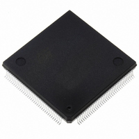
ST10F272Z2Q3 STMicroelectronics, ST10F272Z2Q3 Datasheet - Page 159

ST10F272Z2Q3
Manufacturer Part Number
ST10F272Z2Q3
Description
MCU 16BIT 256KB FLASH 144-PQFP
Manufacturer
STMicroelectronics
Series
ST10r
Datasheet
1.ST10F272Z2Q3.pdf
(189 pages)
Specifications of ST10F272Z2Q3
Core Processor
ST10
Core Size
16-Bit
Speed
64MHz
Connectivity
ASC, CAN, EBI/EMI, I²C, SSC, UART/USART
Peripherals
POR, PWM, WDT
Number Of I /o
111
Program Memory Size
256KB (256K x 8)
Program Memory Type
FLASH
Ram Size
20K x 8
Voltage - Supply (vcc/vdd)
4.5 V ~ 5.5 V
Data Converters
A/D 24x10b
Oscillator Type
Internal
Operating Temperature
-40°C ~ 125°C
Package / Case
144-QFP
Lead Free Status / RoHS Status
Lead free / RoHS Compliant
Eeprom Size
-
Other names
497-5579
Available stocks
Company
Part Number
Manufacturer
Quantity
Price
Company:
Part Number:
ST10F272Z2Q3
Manufacturer:
E-CMOS
Quantity:
10 000
Company:
Part Number:
ST10F272Z2Q3
Manufacturer:
STMicroelectronics
Quantity:
10 000
- Current page: 159 of 189
- Download datasheet (4Mb)
ST10F272Z2
Table 71.
25.8.9
0
0
0
0
(P0H.7-5)
P0.15-13
1
1
0
0
1
0
1
0
Internal PLL divider mechanism (continued)
The PLL input frequency range is limited to 1 to 3.5 MHz, while the VCO oscillation range is
64 to 128 MHz. The CPU clock frequency range when PLL is used is 16 to 64 MHz.
Example 1
●
●
●
●
●
●
Example 2
●
●
●
●
●
●
PLL Jitter
The following terminology is hereafter defined:
●
●
Jitter at the PLL output can be due to the following reasons:
●
●
4 to 12 MHz
4 to 6.4 MHz
1 to 64 MHz
Frequency
f
P0(15:13) = ‘110’ (multiplication by 3)
PLL input frequency = 2.5 MHz
VCO frequency = 120 MHz
PLL output frequency = 30 MHz
(VCO frequency divided by 4)
f
f
P0(15:13) = ‘100’ (Multiplication by 5)
PLL input frequency = 2 MHz
VCO frequency = 80 MHz
PLL output frequency = 40 MHz (VCO frequency divided by 2)
f
Self referred single period jitter
Also called “Period Jitter”, it can be defined as the difference of the T
where T
time period of the PLL output clock.
Self referred long term jitter
Also called “N period jitter”, it can be defined as the difference of T
T
minimum time difference between N+1 clock rising edges. Here N should be kept
sufficiently large to have the long term jitter. For N=1, this becomes the single period
jitter.
Jitter in the input clock
Noise in the PLL loop.
XTAL
CPU
XTAL
CPU
4 MHz
max
XTAL
= 30 MHz (no effect of output prescaler)
= 40 MHz (no effect of Output Prescaler)
is the maximum time difference between N+1 clock rising edges and T
= 10 MHz
= 8 MHz
max
1)
is maximum time period of the PLL output clock and T
Prescaler
F
F
XTAL
XTAL
Input
–
–
/ 2
/ 2
Multiply by
40
64
PLL bypassed
PLL bypassed
PLL
Divide by
2
2
Prescaler
F
Output
PLL
–
–
–
Electrical characteristics
/ 2
max
min
max
CPU Frequency
f
is the minimum
and T
CPU
F
F
and T
F
F
XTAL
XTAL
XTAL
= f
XTAL
min
min
XTAL
x 10
x 16
x 1
min
/ 2
, where
is the
159/189
x F
,
Related parts for ST10F272Z2Q3
Image
Part Number
Description
Manufacturer
Datasheet
Request
R

Part Number:
Description:
STMicroelectronics [RIPPLE-CARRY BINARY COUNTER/DIVIDERS]
Manufacturer:
STMicroelectronics
Datasheet:

Part Number:
Description:
STMicroelectronics [LIQUID-CRYSTAL DISPLAY DRIVERS]
Manufacturer:
STMicroelectronics
Datasheet:

Part Number:
Description:
BOARD EVAL FOR MEMS SENSORS
Manufacturer:
STMicroelectronics
Datasheet:

Part Number:
Description:
NPN TRANSISTOR POWER MODULE
Manufacturer:
STMicroelectronics
Datasheet:

Part Number:
Description:
TURBOSWITCH ULTRA-FAST HIGH VOLTAGE DIODE
Manufacturer:
STMicroelectronics
Datasheet:

Part Number:
Description:
Manufacturer:
STMicroelectronics
Datasheet:

Part Number:
Description:
DIODE / SCR MODULE
Manufacturer:
STMicroelectronics
Datasheet:

Part Number:
Description:
DIODE / SCR MODULE
Manufacturer:
STMicroelectronics
Datasheet:

Part Number:
Description:
Search -----> STE16N100
Manufacturer:
STMicroelectronics
Datasheet:

Part Number:
Description:
Search ---> STE53NA50
Manufacturer:
STMicroelectronics
Datasheet:

Part Number:
Description:
NPN Transistor Power Module
Manufacturer:
STMicroelectronics
Datasheet:


