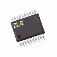
Z8F0413HH005EG Zilog, Z8F0413HH005EG Datasheet - Page 212

Z8F0413HH005EG
Manufacturer Part Number
Z8F0413HH005EG
Description
IC ENCORE MCU FLASH 4K 20SSOP
Manufacturer
Zilog
Series
Encore!® XP®r
Datasheet
1.Z8F0223SB005SG.pdf
(247 pages)
Specifications of Z8F0413HH005EG
Core Processor
Z8
Core Size
8-Bit
Speed
5MHz
Connectivity
IrDA, UART/USART
Peripherals
Brown-out Detect/Reset, LED, POR, PWM, WDT
Number Of I /o
16
Program Memory Size
4KB (4K x 8)
Program Memory Type
FLASH
Ram Size
1K x 8
Voltage - Supply (vcc/vdd)
2.7 V ~ 3.6 V
Oscillator Type
Internal
Operating Temperature
-40°C ~ 105°C
Package / Case
20-SSOP
For Use With
770-1002 - ISP 4PORT ZILOG Z8 ENCORE! MCU269-4643 - KIT DEV Z8 ENCORE XP 28-PIN269-4630 - DEV KIT FOR Z8 ENCORE 8K/4K269-4629 - KIT DEV Z8 ENCORE XP 28-PIN269-4628 - KIT DEV Z8 ENCORE XP 8-PIN
Lead Free Status / RoHS Status
Lead free / RoHS Compliant
Eeprom Size
-
Data Converters
-
Other names
269-4108
Z8F0413HH005EG
Z8F0413HH005EG
- Current page: 212 of 247
- Download datasheet (4Mb)
Table 125. Analog-to-Digital Converter Electrical Characteristics and Timing (Continued)
Symbol Parameter
Zin
Vin
Notes
Symbol Parameter
V
V
T
V
V
Table 126. Comparator Electrical Characteristics
PS024314-0308
1. Analog source impedance affects the ADC offset voltage (because of pin leakage) and input settling time.
2. Devices are factory calibrated at V DD = 3.3 V and T A = +30 °C, so the ADC is maximally accurate under these
3. LSBs are defined assuming 10-bit resolution.
4. This is the maximum recommended resistance seen by the ADC input pin.
5. The input impedance is inversely proportional to the system clock frequency.
PROP
OS
CREF
HYS
IN
conditions.
General Purpose I/O Port Input Data Sample Timing
Input Impedance
Input Voltage Range
Input DC Offset
Programmable Internal
Reference Voltage
Propagation Delay
Input Hysteresis
Input Voltage Range
Figure 29
Port pin is sampled on the rising edge of the system clock. The Port value is available to
the eZ8 CPU on the second rising clock edge following the change of the Port value.
displays timing of the GPIO Port input sampling. The input value on a GPIO
Minimum Typical
Minimum Typical
(unless otherwise stated)
–
0
V
V
T
SS
DD
T
A
V
A
= 0 °C to +70 °C
DD
= 3.0 V to 3.6 V
= -40 °C to +105 °C
= 2.7 V to 3.6 V
150
200
+5
+3
5
4
Maximum
Maximum
V
DD
V
DD
-1
Z8 Encore! XP
Units Conditions
kΩ
V
Units Conditions
mV
mV
ns
%
%
V
Product Specification
In unbuffered mode at 20
MHz
Unbuffered Mode
Electrical Characteristics
20-/28-pin devices
8-pin devices
5
®
F0823 Series
202
Related parts for Z8F0413HH005EG
Image
Part Number
Description
Manufacturer
Datasheet
Request
R

Part Number:
Description:
Communication Controllers, ZILOG INTELLIGENT PERIPHERAL CONTROLLER (ZIP)
Manufacturer:
Zilog, Inc.
Datasheet:

Part Number:
Description:
KIT DEV FOR Z8 ENCORE 16K TO 64K
Manufacturer:
Zilog
Datasheet:

Part Number:
Description:
KIT DEV Z8 ENCORE XP 28-PIN
Manufacturer:
Zilog
Datasheet:

Part Number:
Description:
DEV KIT FOR Z8 ENCORE 8K/4K
Manufacturer:
Zilog
Datasheet:

Part Number:
Description:
KIT DEV Z8 ENCORE XP 28-PIN
Manufacturer:
Zilog
Datasheet:

Part Number:
Description:
DEV KIT FOR Z8 ENCORE 4K TO 8K
Manufacturer:
Zilog
Datasheet:

Part Number:
Description:
CMOS Z8 microcontroller. ROM 16 Kbytes, RAM 256 bytes, speed 16 MHz, 32 lines I/O, 3.0V to 5.5V
Manufacturer:
Zilog, Inc.
Datasheet:

Part Number:
Description:
Low-cost microcontroller. 512 bytes ROM, 61 bytes RAM, 8 MHz
Manufacturer:
Zilog, Inc.
Datasheet:

Part Number:
Description:
Z8 4K OTP Microcontroller
Manufacturer:
Zilog, Inc.
Datasheet:

Part Number:
Description:
CMOS SUPER8 ROMLESS MCU
Manufacturer:
Zilog, Inc.
Datasheet:

Part Number:
Description:
SL1866 CMOSZ8 OTP Microcontroller
Manufacturer:
Zilog, Inc.
Datasheet:

Part Number:
Description:
SL1866 CMOSZ8 OTP Microcontroller
Manufacturer:
Zilog, Inc.
Datasheet:

Part Number:
Description:
OTP (KB) = 1, RAM = 125, Speed = 12, I/O = 14, 8-bit Timers = 2, Comm Interfaces Other Features = Por, LV Protect, Voltage = 4.5-5.5V
Manufacturer:
Zilog, Inc.
Datasheet:

Part Number:
Description:
Manufacturer:
Zilog, Inc.
Datasheet:


