T89C5115-TISUM Atmel, T89C5115-TISUM Datasheet - Page 6
T89C5115-TISUM
Manufacturer Part Number
T89C5115-TISUM
Description
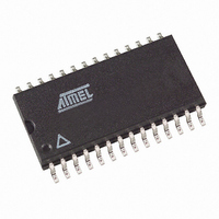
IC 8051 MCU FLASH 16K 28SOIC
Manufacturer
Atmel
Series
89Cr
Datasheet
1.T89C5115-RATIM.pdf
(113 pages)
Specifications of T89C5115-TISUM
Core Processor
8051
Core Size
8-Bit
Speed
40MHz
Connectivity
UART/USART
Peripherals
POR, PWM, WDT
Number Of I /o
20
Program Memory Size
16KB (16K x 8)
Program Memory Type
FLASH
Eeprom Size
2K x 8
Ram Size
512 x 8
Voltage - Supply (vcc/vdd)
3 V ~ 5.5 V
Data Converters
A/D 8x10b
Oscillator Type
Internal
Operating Temperature
-40°C ~ 85°C
Package / Case
28-SOIC (7.5mm Width)
Lead Free Status / RoHS Status
Lead free / RoHS Compliant
Other names
89C5115-TISUM


6
Pin Name
RESET
XTAL1
XTAL2
P3.0:7
P4.0:1
AT89C5115
Type
I/O
I/O
I/O
O
I
Description
Port 3:
Is an 8-bit bi-directional I/O port with internal pull-ups. Port 3 pins that have 1’s written to them are pulled
high by the internal pull-up transistors and can be used as inputs in this state. As inputs, Port 3 pins that
are being pulled low externally will be a source of current (I
because of the internal pull-ups.
The output latch corresponding to a secondary function must be programmed to one for that function to
operate (except for TxD and WR). The secondary functions are assigned to the pins of port 3 as follows:
P3.0/RxD: Receiver data input (asynchronous) or data input/output (synchronous) of the serial interface
P3.1/TxD: Transmitter data output (asynchronous) or clock output (synchronous) of the serial interface
P3.2/INT0: External interrupt 0 input/timer 0 gate control input
P3.3/INT1: External interrupt 1 input/timer 1 gate control input
P3.4/T0: Timer 0 counter input
P3.5/T1: Timer 1 counter input
P3.6: Regular I/O port pin
P3.7: Regular I/O port pin
Port 4:
Is an 2-bit bi-directional I/O port with internal pull-ups. Port 4 pins that have 1’s written to them are pulled
high by the internal pull-ups and can be used as inputs in this state. As inputs, Port 4 pins that are being
pulled low externally will be a source of current (IIL, on the datasheet) because of the internal pull-up
transistor.
P4.0:
P4.1:
It can drive CMOS inputs without external pull-ups.
Reset:
A high level on this pin during two machine cycles while the oscillator is running resets the device. An
internal pull-down resistor to VSS permits power-on reset using only an external capacitor to VCC.
XTAL1:
Input of the inverting oscillator amplifier and input of the internal clock generator circuits. To drive the
device from an external clock source, XTAL1 should be driven, while XTAL2 is left unconnected. To
operate above a frequency of 16 MHz, a duty cycle of 50% should be maintained.
XTAL2:
Output from the inverting oscillator amplifier.
IL
, See section ’Electrical Characteristic’)
4128G–8051–02/08
Related parts for T89C5115-TISUM
Image
Part Number
Description
Manufacturer
Datasheet
Request
R

Part Number:
Description:
IC 8051 MCU FLASH 16K 32VQFP
Manufacturer:
Atmel
Datasheet:

Part Number:
Description:
IC 8051 MCU FLASH 16K 28PLCC
Manufacturer:
Atmel
Datasheet:

Part Number:
Description:
IC 8051 MCU FLASH 16K 24SOIC
Manufacturer:
Atmel
Datasheet:

Part Number:
Description:
IC 8051 MCU FLASH 16K 28SOIC
Manufacturer:
Atmel
Datasheet:

Part Number:
Description:
Low Pin Count 8-bit MCU with A/D Converter and 16-Kbytes of Flash Memory
Manufacturer:
ATMEL Corporation
Datasheet:

Part Number:
Description:
DEV KIT FOR AVR/AVR32
Manufacturer:
Atmel
Datasheet:
Part Number:
Description:
INTERVAL AND WIPE/WASH WIPER CONTROL IC WITH DELAY
Manufacturer:
ATMEL Corporation
Datasheet:
Part Number:
Description:
Low-Voltage Voice-Switched IC for Hands-Free Operation
Manufacturer:
ATMEL Corporation
Datasheet:
Part Number:
Description:
MONOLITHIC INTEGRATED FEATUREPHONE CIRCUIT
Manufacturer:
ATMEL Corporation
Datasheet:
Part Number:
Description:
AM-FM Receiver IC U4255BM-M
Manufacturer:
ATMEL Corporation
Datasheet:
Part Number:
Description:
Monolithic Integrated Feature Phone Circuit
Manufacturer:
ATMEL Corporation
Datasheet:
Part Number:
Description:
Multistandard Video-IF and Quasi Parallel Sound Processing
Manufacturer:
ATMEL Corporation
Datasheet: