T89C5115-TISUM Atmel, T89C5115-TISUM Datasheet - Page 5
T89C5115-TISUM
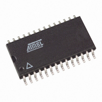
Manufacturer Part Number
T89C5115-TISUM
Description
IC 8051 MCU FLASH 16K 28SOIC
Manufacturer
Atmel
Series
89Cr
Datasheet
1.T89C5115-RATIM.pdf
(113 pages)
Specifications of T89C5115-TISUM
Core Processor
8051
Core Size
8-Bit
Speed
40MHz
Connectivity
UART/USART
Peripherals
POR, PWM, WDT
Number Of I /o
20
Program Memory Size
16KB (16K x 8)
Program Memory Type
FLASH
Eeprom Size
2K x 8
Ram Size
512 x 8
Voltage - Supply (vcc/vdd)
3 V ~ 5.5 V
Data Converters
A/D 8x10b
Oscillator Type
Internal
Operating Temperature
-40°C ~ 85°C
Package / Case
28-SOIC (7.5mm Width)
Lead Free Status / RoHS Status
Lead free / RoHS Compliant
Other names
89C5115-TISUM


Pin Description
4128G–8051–02/08
Pin Name
VAGND
VAREF
VAVCC
P1.0:7
P2.0:1
VSS
VCC
GND
Type
I/O
I/O
Description
Circuit ground
Supply Voltage
Reference Voltage for ADC
Supply Voltage for ADC
Reference Ground for ADC
Port 1:
Is an 8-bit bi-directional I/O port with internal pull-ups. Port 1 pins can be used for digital input/output or as
analog inputs for the Analog Digital Converter (ADC). Port 1 pins that have 1’s written to them are pulled
high by the internal pull-up transistors and can be used as inputs in this state. As inputs, Port 1 pins that
are being pulled low externally will be the source of current (I
because of the internal pull-ups. Port 1 pins are assigned to be used as analog inputs via the ADCCF
register (in this case the internal pull-ups are disconnected).
As a secondary digital function, port 1 contains the Timer 2 external trigger and clock input; the PCA
external clock input and the PCA module I/O.
P1.0/AN0/T2
Analog input channel 0,
External clock input for Timer/counter2.
P1.1/AN1/T2EX
Analog input channel 1,
Trigger input for Timer/counter2.
P1.2/AN2/ECI
Analog input channel 2,
PCA external clock input.
P1.3/AN3/CEX0
Analog input channel 3,
PCA module 0 Entry of input/PWM output.
P1.4/AN4/CEX1
Analog input channel 4,
PCA module 1 Entry of input/PWM output.
P1.5/AN5
Analog input channel 5,
P1.6/AN6
Analog input channel 6,
P1.7/AN7
Analog input channel 7,
It can drive CMOS inputs without external pull-ups.
Port 2:
Is an 2-bit bi-directional I/O port with internal pull-ups. Port 2 pins that have 1’s written to them are pulled
high by the internal pull-ups and can be used as inputs in this state. As inputs, Port 2 pins that are being
pulled low externally will be a source of current (IIL, on the datasheet) because of the internal pull-ups.
In the T89C5115 Port 2 can sink or source 5mA. It can drive CMOS inputs without external pull-ups.
IL
, See section ’Electrical Characteristic’)
5
Related parts for T89C5115-TISUM
Image
Part Number
Description
Manufacturer
Datasheet
Request
R

Part Number:
Description:
IC 8051 MCU FLASH 16K 32VQFP
Manufacturer:
Atmel
Datasheet:

Part Number:
Description:
IC 8051 MCU FLASH 16K 28PLCC
Manufacturer:
Atmel
Datasheet:

Part Number:
Description:
IC 8051 MCU FLASH 16K 24SOIC
Manufacturer:
Atmel
Datasheet:

Part Number:
Description:
IC 8051 MCU FLASH 16K 28SOIC
Manufacturer:
Atmel
Datasheet:

Part Number:
Description:
Low Pin Count 8-bit MCU with A/D Converter and 16-Kbytes of Flash Memory
Manufacturer:
ATMEL Corporation
Datasheet:

Part Number:
Description:
DEV KIT FOR AVR/AVR32
Manufacturer:
Atmel
Datasheet:
Part Number:
Description:
INTERVAL AND WIPE/WASH WIPER CONTROL IC WITH DELAY
Manufacturer:
ATMEL Corporation
Datasheet:
Part Number:
Description:
Low-Voltage Voice-Switched IC for Hands-Free Operation
Manufacturer:
ATMEL Corporation
Datasheet:
Part Number:
Description:
MONOLITHIC INTEGRATED FEATUREPHONE CIRCUIT
Manufacturer:
ATMEL Corporation
Datasheet:
Part Number:
Description:
AM-FM Receiver IC U4255BM-M
Manufacturer:
ATMEL Corporation
Datasheet:
Part Number:
Description:
Monolithic Integrated Feature Phone Circuit
Manufacturer:
ATMEL Corporation
Datasheet:
Part Number:
Description:
Multistandard Video-IF and Quasi Parallel Sound Processing
Manufacturer:
ATMEL Corporation
Datasheet: