R5F21134DFP#U0 Renesas Electronics America, R5F21134DFP#U0 Datasheet - Page 77
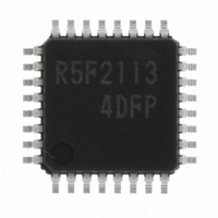
R5F21134DFP#U0
Manufacturer Part Number
R5F21134DFP#U0
Description
IC R8C MCU FLASH 32LQFP
Manufacturer
Renesas Electronics America
Series
M16C™ M16C/R8C/Tiny/13r
Datasheets
1.R5F211A2SPU0.pdf
(300 pages)
2.R5F21132FPU0.pdf
(33 pages)
3.R5F21132FPU0.pdf
(226 pages)
4.R5F21134DFPU0.pdf
(224 pages)
Specifications of R5F21134DFP#U0
Core Size
16-Bit
Program Memory Size
16KB (16K x 8)
Oscillator Type
Internal
Core Processor
R8C
Speed
20MHz
Connectivity
SIO, UART/USART
Peripherals
LED, POR, Voltage Detect, WDT
Number Of I /o
22
Program Memory Type
FLASH
Ram Size
1K x 8
Voltage - Supply (vcc/vdd)
2.7 V ~ 5.5 V
Data Converters
A/D 12x10b
Operating Temperature
-40°C ~ 85°C
Package / Case
32-LQFP
No. Of I/o's
22
Eeprom Memory Size
4KB
Ram Memory Size
1024Byte
Cpu Speed
20MHz
No. Of Timers
16
Digital Ic Case
RoHS Compliant
Controller Family/series
R8C/13
Rohs Compliant
Yes
Lead Free Status / RoHS Status
Lead free / RoHS Compliant
For Use With
R0K521134S000BE - KIT EVAL STARTER FOR R8C/13R0E521134EPB00 - KIT EMULATOR PROBE FOR PC7501R0E521134CPE00 - EMULATOR COMPACT R8C/13
Eeprom Size
-
Lead Free Status / RoHS Status
Lead free / RoHS Compliant
Available stocks
Company
Part Number
Manufacturer
Quantity
Price

Part Number:
R5F21134DFP#U0R5F21134DFP
Manufacturer:
Renesas Electronics America
Quantity:
10 000


R8C/13 Group
Rev.1.20
REJ09B0111-0120
Figure 10.14 TCC0 Register and TCC1 Register
T i m e r C c o n t r o l r e g i s t e r 0
b 7 b 6 b 5 b4 b 3 b 2 b 1 b 0
NOTES:
Jan 27, 2006
1. Change this bit when TCC00 bit is set to “0” (count stop).
2. The IR bit in the INT3IC may be set to “1” (interrupt requested) when the TCC03, TCC04, or TCC07 bit is rewritten.
Timer C control register 1
b 7 b 6 b 5 b 4 b 3 b 2 b 1 b 0
0 0
Refer to the paragraph 19.2.5 “Changing Interrupt Factir” in the Usage Notes Reference Book.
N O T E S :
1 . I n p u t i s r e c o g n i z e d o n l y w h e n t h e s a m e v a l u e f r o m I N T 3 p i n i s s a m p l e d t h r e e t i m e s i n s u c c e s s i o n .
2 . M o d i f y t h e T C C 1 3 b i t w h e n t h e T C C 0 0 b i t i n t h e T C C 0 r e g i s t e r i s s e t t o “ 0 ” ( c o u n t s t o p s )
3 . S e t t h e T C C 1 2 , T C C 1 4 t o T C C 1 7 b i t s t o “ 0 ” w h e n t h e T C C 1 3 b i t i s s e t t o “ 0 ” ( i n p u t c a p t u r e m o d e ) .
page 64 of 205
Bit symbol
B i t s y m b o l
TCC07
T C C 0 0
T C C 0 1
T C C 0 2
T C C 0 3
T C C 0 4
( b 6 - b 5 )
T C C 1 0
T C C 1 1
T C C 1 6
T C C 1 7
T C C 1 2
T C C 1 3
T C C 1 4
T C C 1 5
S y m b o l
T C C 0
S y m b o l
T C C 1
I N T 3 i n t e r r u p t / c a p t u r e i n p u t
s w i t c h i n g b i t
Timer C control bit
Timer C count source select
bit
INT3 interrupt and capture
polarity select bit
R e s e r v e d b i t
I N T 3 i n p u t f i l t e r s e l e c t b i t
C o m p a r e 1 o u t p u t m o d e
s e l e c t b i t
Timer C counter reload
select bit
Compare 0/Capture select
bit
Compare 0 output mode
select bit
(1)
(3 )
B i t n a m e
(2, 3)
(3)
Bit name
(1 , 2 )
A d d r e s s
A d d r e s s
0 0 9 A
0 0 9 B
(1, 2)
1 6
1 6
(1 )
A f t e r r e s e t
A f t e r r e s e t
0 0: CMP output remains unchanged
0 1: CMP output is reversed when
1 0: CMP output is set to low when
1 1: CMP output is set to high when
b 5 b 4
0 : I N T 3
1 : f
b 1 b 0
0 0: CMP output remains unchanged
0 1: CMP output is reversed when
1 0: CMP output is set to low when
1 1: CMP output is set to high when
0 : C o u n t s t o p
1 : C o u n t s t a r t
b 2 b 1
0 0 : f
0 1 : f
1 0 : f
1 1 : f
0 0
0 0 : N o f i l t e r
0 1 : F i l t e r w i t h f
1 0 : F i l t e r w i t h f
1 1 : F i l t e r w i t h f
b4 b3
0 0 : Rising edge
0 1 : Falling edge
1 0 : Both edges
1 1 : Avoid this setting
0: No reload (free-run)
1: Set TC register to “0000
0: Capture
1: Compare 0 output
b 7 b 6
0 0
S e t t o " 0 "
(input capture mode)
(output compare mode)
1 6
compare 1 match
1 6
R I N G 1 2 8
even when compare 0 matched
compare 0 signal is matched
compare 0 signal is matched
compare 0 signal is matched
even when compare 1 matched
compare 1 signal is matched
compare 1 signal is matched
compare 1 signal is matched
1
8
3 2
R I N G
- f a s t
Function
F u n c t i o n
1
8
3 2
s a m p l i n g
s a m p l i n g
s a m p l i n g
(2)
16
” at
R W
RW
RW
RW
RW
R W
RO
10.2 INT Interrupt
R W
R W
R W
R W
R W
R W
R W
R W
______
Related parts for R5F21134DFP#U0
Image
Part Number
Description
Manufacturer
Datasheet
Request
R

Part Number:
Description:
KIT STARTER FOR M16C/29
Manufacturer:
Renesas Electronics America
Datasheet:

Part Number:
Description:
KIT STARTER FOR R8C/2D
Manufacturer:
Renesas Electronics America
Datasheet:

Part Number:
Description:
R0K33062P STARTER KIT
Manufacturer:
Renesas Electronics America
Datasheet:

Part Number:
Description:
KIT STARTER FOR R8C/23 E8A
Manufacturer:
Renesas Electronics America
Datasheet:

Part Number:
Description:
KIT STARTER FOR R8C/25
Manufacturer:
Renesas Electronics America
Datasheet:

Part Number:
Description:
KIT STARTER H8S2456 SHARPE DSPLY
Manufacturer:
Renesas Electronics America
Datasheet:

Part Number:
Description:
KIT STARTER FOR R8C38C
Manufacturer:
Renesas Electronics America
Datasheet:

Part Number:
Description:
KIT STARTER FOR R8C35C
Manufacturer:
Renesas Electronics America
Datasheet:

Part Number:
Description:
KIT STARTER FOR R8CL3AC+LCD APPS
Manufacturer:
Renesas Electronics America
Datasheet:
Part Number:
Description:
KIT STARTER FOR RX610
Manufacturer:
Renesas Electronics America
Datasheet:

Part Number:
Description:
KIT STARTER FOR R32C/118
Manufacturer:
Renesas Electronics America
Datasheet:

Part Number:
Description:
KIT DEV RSK-R8C/26-29
Manufacturer:
Renesas Electronics America
Datasheet:

Part Number:
Description:
KIT STARTER FOR SH7124
Manufacturer:
Renesas Electronics America
Datasheet:

Part Number:
Description:
KIT STARTER FOR H8SX/1622
Manufacturer:
Renesas Electronics America
Datasheet:

Part Number:
Description:
KIT DEV FOR SH7203
Manufacturer:
Renesas Electronics America
Datasheet: