R5F21122FP#U0 Renesas Electronics America, R5F21122FP#U0 Datasheet - Page 9
R5F21122FP#U0
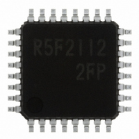
Manufacturer Part Number
R5F21122FP#U0
Description
IC R8C MCU FLASH 8K 32LQFP
Manufacturer
Renesas Electronics America
Series
M16C™ M16C/R8C/Tiny/12r
Datasheets
1.R5F211A2SPU0.pdf
(300 pages)
2.R5F21122FPU0.pdf
(30 pages)
3.R5F21122FPU0.pdf
(200 pages)
Specifications of R5F21122FP#U0
Core Processor
R8C
Core Size
16-Bit
Speed
16MHz
Connectivity
SIO, UART/USART
Peripherals
LED, WDT
Number Of I /o
22
Program Memory Size
8KB (8K x 8)
Program Memory Type
FLASH
Ram Size
512 x 8
Voltage - Supply (vcc/vdd)
2.7 V ~ 5.5 V
Data Converters
A/D 8x10b
Oscillator Type
Internal
Operating Temperature
-20°C ~ 85°C
Package / Case
32-LQFP
For Use With
R0K521134S000BE - KIT EVAL STARTER FOR R8C/13R0E521134EPB00 - KIT EMULATOR PROBE FOR PC7501R0E521134CPE00 - EMULATOR COMPACT R8C/13
Lead Free Status / RoHS Status
Lead free / RoHS Compliant
Eeprom Size
-
Available stocks
Company
Part Number
Manufacturer
Quantity
Price


12.3 Timer Z ........................................................................................................................... 73
12.4 Timer C ........................................................................................................................... 86
Chapter 13. Serial Interface ................................................ 89
Chapter 14. A/D Converter................................................ 104
Chapter 15. Programmable I/O Ports .............................. 116
Chapter 16. Electrical Characteristics ............................. 130
Chapter 17. Flash Memory Version ................................. 141
13.1 Clock Synchronous Serial I/O Mode ......................................................................... 94
13.2 Clock Asynchronous Serial I/O (UART) Mode ......................................................... 99
14.1 One-shot Mode ......................................................................................................... 108
14.2 Repeat Mode ............................................................................................................. 109
14.3 Sample & Hold .......................................................................................................... 111
14.4 A/D conversion cycles ........................................................................................... 111
14.5 Internal Equivalent Circuit of Analog Input ........................................................... 112
14.6 Inflow Current Bypass Circuit ................................................................................ 113
14.7 Output Impedance of Sensor under A/D Conversion........................................... 114
15. 1 Description ............................................................................................................... 116
15.2 Port setting ................................................................................................................ 123
15.3 Unassigned Pin Handling ........................................................................................ 129
17.1 Overview .................................................................................................................... 141
17.2 Memory Map .............................................................................................................. 142
17.3 Functions To Prevent Flash Memory from Rewriting............................................ 143
17.4 CPU Rewrite Mode .................................................................................................... 144
12.3.1 Timer Mode .......................................................................................................................................... 76
12.3.2 Programmable Waveform Generation Mode .................................................................................... 78
12.3.3 Programmable One-shot Generation Mode ...................................................................................... 80
12.3.4 Programmable Wait One-shot Generation Mode ............................................................................. 83
13.1.1 Polarity Select Function ..................................................................................................................... 97
13.1.2 LSB First/MSB First Select Function ................................................................................................ 97
13.1.3 Continuous Receive Mode ................................................................................................................. 98
13.2.1 TxD10/RxD1 Select Function (UART1) ............................................................................................ 102
13.2.2 TxD11 Select Function (UART1) ...................................................................................................... 102
13.2.3 Bit Rate .............................................................................................................................................. 103
15.1.1 Port Pi Direction Register (PDi Register, i = 0, 1, 3, 4) ................................................................... 116
15.1.2 Port Pi Register (Pi Register, i = 0 to 4)........................................................................................... 116
15.1.3 Pull-up Control Register 0, Pull-up Control Register 1 (PUR0 and PUR1 Registers) ................. 116
15.1.4 Port P1 Drive Capacity Control Register (DRR Register) .............................................................. 116
17.3.1 ID Code Check Function .................................................................................................................. 143
17.4.1 EW0 Mode .......................................................................................................................................... 145
17.4.2 EW1 Mode .......................................................................................................................................... 145
17.4.3 Software Commands ........................................................................................................................ 151
17.4.4 Status Register .................................................................................................................................. 155
17.4.5 Full Status Check .............................................................................................................................. 156
A-3
Related parts for R5F21122FP#U0
Image
Part Number
Description
Manufacturer
Datasheet
Request
R

Part Number:
Description:
KIT STARTER FOR M16C/29
Manufacturer:
Renesas Electronics America
Datasheet:

Part Number:
Description:
KIT STARTER FOR R8C/2D
Manufacturer:
Renesas Electronics America
Datasheet:

Part Number:
Description:
R0K33062P STARTER KIT
Manufacturer:
Renesas Electronics America
Datasheet:

Part Number:
Description:
KIT STARTER FOR R8C/23 E8A
Manufacturer:
Renesas Electronics America
Datasheet:

Part Number:
Description:
KIT STARTER FOR R8C/25
Manufacturer:
Renesas Electronics America
Datasheet:

Part Number:
Description:
KIT STARTER H8S2456 SHARPE DSPLY
Manufacturer:
Renesas Electronics America
Datasheet:

Part Number:
Description:
KIT STARTER FOR R8C38C
Manufacturer:
Renesas Electronics America
Datasheet:

Part Number:
Description:
KIT STARTER FOR R8C35C
Manufacturer:
Renesas Electronics America
Datasheet:

Part Number:
Description:
KIT STARTER FOR R8CL3AC+LCD APPS
Manufacturer:
Renesas Electronics America
Datasheet:
Part Number:
Description:
KIT STARTER FOR RX610
Manufacturer:
Renesas Electronics America
Datasheet:

Part Number:
Description:
KIT STARTER FOR R32C/118
Manufacturer:
Renesas Electronics America
Datasheet:

Part Number:
Description:
KIT DEV RSK-R8C/26-29
Manufacturer:
Renesas Electronics America
Datasheet:

Part Number:
Description:
KIT STARTER FOR SH7124
Manufacturer:
Renesas Electronics America
Datasheet:

Part Number:
Description:
KIT STARTER FOR H8SX/1622
Manufacturer:
Renesas Electronics America
Datasheet:

Part Number:
Description:
KIT DEV FOR SH7203
Manufacturer:
Renesas Electronics America
Datasheet: