R5F21122FP#U0 Renesas Electronics America, R5F21122FP#U0 Datasheet - Page 26
R5F21122FP#U0
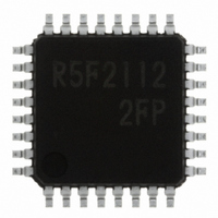
Manufacturer Part Number
R5F21122FP#U0
Description
IC R8C MCU FLASH 8K 32LQFP
Manufacturer
Renesas Electronics America
Series
M16C™ M16C/R8C/Tiny/12r
Datasheets
1.R5F211A2SPU0.pdf
(300 pages)
2.R5F21122FPU0.pdf
(30 pages)
3.R5F21122FPU0.pdf
(200 pages)
Specifications of R5F21122FP#U0
Core Processor
R8C
Core Size
16-Bit
Speed
16MHz
Connectivity
SIO, UART/USART
Peripherals
LED, WDT
Number Of I /o
22
Program Memory Size
8KB (8K x 8)
Program Memory Type
FLASH
Ram Size
512 x 8
Voltage - Supply (vcc/vdd)
2.7 V ~ 5.5 V
Data Converters
A/D 8x10b
Oscillator Type
Internal
Operating Temperature
-20°C ~ 85°C
Package / Case
32-LQFP
For Use With
R0K521134S000BE - KIT EVAL STARTER FOR R8C/13R0E521134EPB00 - KIT EMULATOR PROBE FOR PC7501R0E521134CPE00 - EMULATOR COMPACT R8C/13
Lead Free Status / RoHS Status
Lead free / RoHS Compliant
Eeprom Size
-
Available stocks
Company
Part Number
Manufacturer
Quantity
Price


R8C/12 Group
Rev.1.20
REJ09B0110-0120
Table 5.1 Pin Status When RESET Pin Level is “L”
P0
P3
P4
5. Reset
P1
0
5 to
5.2 Software Reset
5.3 Watchdog Timer Reset
There are three types of resets: a hardware reset, a software reset, and an watchdog timer reset.
5.1 Hardware Reset
Pin name
to P3
P4
Jan 27, 2006
the reset vector. After reset, the on-chip oscillator clock divided by 8 is automatically selected for the
Where the PM12 bit in the PM1 register is “1” (reset when watchdog timer underflows), the microcom-
puter initializes its pins, CPU and SFR if the watchdog timer underflows. Then the program is ex-
ecuted starting from the address indicated by the reset vector. After reset, the on-chip oscillator clock
divided by 8 is automatically selected for the CPU.
pins, CPU, and SFR initialized. Then the program is executed starting from the address indicated by
When the PM03 bit in the PM0 register is set to “1” (microcomputer reset), the microcomputer has its
CPU.
7
3
A reset is applied using the RESET pin. When an “L” signal is applied to the RESET pin while
the power supply voltage is within the recommended operating condition, the pins are initial-
ized (see Table 5.1 “Pin Status When RESET Pin Level is 'L'”). When the input level at the
____________
RESET pin is released from “L” to “H”, the CPU and SFR are initialized, and the program is
executed starting from the address indicated by the reset vector. Figure 5.1 shows the CPU
register status after reset and figure 5.2 shows the reset sequence. After reset, the on-chip
oscillator clock divided by 8 is automatically selected for the CPU. The internal RAM is not
initialized. If the RESET pin is pulled “L” while writing to the internal RAM, the internal RAM
becomes indeterminate. Figures 5.3 to 5.4 show the reset circuit example. Refer to Chapter 4,
“Special Function Register (SFR)” for the status of SFR after reset.
• When the power supply is stable
(1) Apply an “L” signal to the RESET pin.
(2) Wait for 500 µs (1/f
(3) Apply an “H” signal to the RESET pin.
• Power on
(1) Apply an “L” signal to the RESET pin.
(2) Let the power supply voltage increase until it meets the recommended operating condition.
(3) Wait td(P-R) or more until the internal power supply stabilizes.
(4) Wait for 500 µs (1/f
(5) Apply an “H” signal to the RESET pin.
, P3
7
Input port
Input port
Input port
Input port
page 14 of 181
____________
Status
____________
RING
RING
____________
____________
____________
____________
____________
20).
20).
____________
____________
5. Reset
Related parts for R5F21122FP#U0
Image
Part Number
Description
Manufacturer
Datasheet
Request
R

Part Number:
Description:
KIT STARTER FOR M16C/29
Manufacturer:
Renesas Electronics America
Datasheet:

Part Number:
Description:
KIT STARTER FOR R8C/2D
Manufacturer:
Renesas Electronics America
Datasheet:

Part Number:
Description:
R0K33062P STARTER KIT
Manufacturer:
Renesas Electronics America
Datasheet:

Part Number:
Description:
KIT STARTER FOR R8C/23 E8A
Manufacturer:
Renesas Electronics America
Datasheet:

Part Number:
Description:
KIT STARTER FOR R8C/25
Manufacturer:
Renesas Electronics America
Datasheet:

Part Number:
Description:
KIT STARTER H8S2456 SHARPE DSPLY
Manufacturer:
Renesas Electronics America
Datasheet:

Part Number:
Description:
KIT STARTER FOR R8C38C
Manufacturer:
Renesas Electronics America
Datasheet:

Part Number:
Description:
KIT STARTER FOR R8C35C
Manufacturer:
Renesas Electronics America
Datasheet:

Part Number:
Description:
KIT STARTER FOR R8CL3AC+LCD APPS
Manufacturer:
Renesas Electronics America
Datasheet:
Part Number:
Description:
KIT STARTER FOR RX610
Manufacturer:
Renesas Electronics America
Datasheet:

Part Number:
Description:
KIT STARTER FOR R32C/118
Manufacturer:
Renesas Electronics America
Datasheet:

Part Number:
Description:
KIT DEV RSK-R8C/26-29
Manufacturer:
Renesas Electronics America
Datasheet:

Part Number:
Description:
KIT STARTER FOR SH7124
Manufacturer:
Renesas Electronics America
Datasheet:

Part Number:
Description:
KIT STARTER FOR H8SX/1622
Manufacturer:
Renesas Electronics America
Datasheet:

Part Number:
Description:
KIT DEV FOR SH7203
Manufacturer:
Renesas Electronics America
Datasheet: