R5F21122FP#U0 Renesas Electronics America, R5F21122FP#U0 Datasheet - Page 7
R5F21122FP#U0
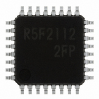
Manufacturer Part Number
R5F21122FP#U0
Description
IC R8C MCU FLASH 8K 32LQFP
Manufacturer
Renesas Electronics America
Series
M16C™ M16C/R8C/Tiny/12r
Datasheets
1.R5F211A2SPU0.pdf
(300 pages)
2.R5F21122FPU0.pdf
(30 pages)
3.R5F21122FPU0.pdf
(200 pages)
Specifications of R5F21122FP#U0
Core Processor
R8C
Core Size
16-Bit
Speed
16MHz
Connectivity
SIO, UART/USART
Peripherals
LED, WDT
Number Of I /o
22
Program Memory Size
8KB (8K x 8)
Program Memory Type
FLASH
Ram Size
512 x 8
Voltage - Supply (vcc/vdd)
2.7 V ~ 5.5 V
Data Converters
A/D 8x10b
Oscillator Type
Internal
Operating Temperature
-20°C ~ 85°C
Package / Case
32-LQFP
For Use With
R0K521134S000BE - KIT EVAL STARTER FOR R8C/13R0E521134EPB00 - KIT EMULATOR PROBE FOR PC7501R0E521134CPE00 - EMULATOR COMPACT R8C/13
Lead Free Status / RoHS Status
Lead free / RoHS Compliant
Eeprom Size
-
Available stocks
Company
Part Number
Manufacturer
Quantity
Price


SFR Page Reference
Chapter 1. Overview ............................................................. 1
Chapter 2. Central Processing Unit (CPU) ......................... 7
Chapter 3. Memory ............................................................... 9
Chapter 4. Special Function Registers (SFR) .................. 10
Chapter 5. Reset .................................................................. 14
Chapter 6. Clock Generation Circuit.................................. 17
1.1 Applications ................................................................................................................... 1
1.2 Performance Overview .................................................................................................. 2
1.3 Block Diagram ............................................................................................................... 3
1.4 Product Information ...................................................................................................... 4
1.5 Pin Assignments ............................................................................................................ 5
1.6 Pin Description .............................................................................................................. 6
2.1 Data Registers (R0, R1, R2 and R3 ) ............................................................................. 7
2.2 AddressRegisters (A0 and A1) ...................................................................................... 8
2.3 Frame Base Register( FB ) ............................................................................................. 8
2.4 Interrupt Table Register (INTB )..................................................................................... 8
2.5 Program Counter (PC ) ................................................................................................... 8
2.6 User Stack Pointer (USP ) and Interrupt Stack Pointer (ISP )..................................... 8
2.7 Static Base Register (SB ) ............................................................................................. 8
2.8 Flag Register (FLG ) ....................................................................................................... 8
5.1 Hardware Reset ............................................................................................................ 14
5.2 Software Reset .............................................................................................................. 14
5.3 Watchdog Timer Reset ................................................................................................. 14
6.1 Main Clock ..................................................................................................................... 21
6.2 On-Chip Oscillator Clock ............................................................................................. 22
2.8.1 Carry Flag ( C Flag ) ................................................................................................................................ 8
2.8.2 Debug Flag ( D Flag ) .............................................................................................................................. 8
2.8.3 Zero Flag ( Z Flag ) .................................................................................................................................. 8
2.8.4 Sign Flag ( S Flag ) .................................................................................................................................. 8
2.8.5 Register Bank Select Flag ( B Flag ) ..................................................................................................... 8
2.8.6 Overflow Flag ( O Flag) ........................................................................................................................... 8
2.8.7 Interrupt Enable Flag ( I Flag ) ............................................................................................................... 8
2.8.8 Stack Pointer Select Flag ( U Flag ) ....................................................................................................... 8
2.8.9 Processor Interrupt Priority Level ( IPL ) .............................................................................................. 8
2.8.10 Reserved Area ....................................................................................................................................... 8
Table of Contents
A-1
Related parts for R5F21122FP#U0
Image
Part Number
Description
Manufacturer
Datasheet
Request
R

Part Number:
Description:
KIT STARTER FOR M16C/29
Manufacturer:
Renesas Electronics America
Datasheet:

Part Number:
Description:
KIT STARTER FOR R8C/2D
Manufacturer:
Renesas Electronics America
Datasheet:

Part Number:
Description:
R0K33062P STARTER KIT
Manufacturer:
Renesas Electronics America
Datasheet:

Part Number:
Description:
KIT STARTER FOR R8C/23 E8A
Manufacturer:
Renesas Electronics America
Datasheet:

Part Number:
Description:
KIT STARTER FOR R8C/25
Manufacturer:
Renesas Electronics America
Datasheet:

Part Number:
Description:
KIT STARTER H8S2456 SHARPE DSPLY
Manufacturer:
Renesas Electronics America
Datasheet:

Part Number:
Description:
KIT STARTER FOR R8C38C
Manufacturer:
Renesas Electronics America
Datasheet:

Part Number:
Description:
KIT STARTER FOR R8C35C
Manufacturer:
Renesas Electronics America
Datasheet:

Part Number:
Description:
KIT STARTER FOR R8CL3AC+LCD APPS
Manufacturer:
Renesas Electronics America
Datasheet:
Part Number:
Description:
KIT STARTER FOR RX610
Manufacturer:
Renesas Electronics America
Datasheet:

Part Number:
Description:
KIT STARTER FOR R32C/118
Manufacturer:
Renesas Electronics America
Datasheet:

Part Number:
Description:
KIT DEV RSK-R8C/26-29
Manufacturer:
Renesas Electronics America
Datasheet:

Part Number:
Description:
KIT STARTER FOR SH7124
Manufacturer:
Renesas Electronics America
Datasheet:

Part Number:
Description:
KIT STARTER FOR H8SX/1622
Manufacturer:
Renesas Electronics America
Datasheet:

Part Number:
Description:
KIT DEV FOR SH7203
Manufacturer:
Renesas Electronics America
Datasheet: